Japan Semiconductor Bonding Market (2026-2032) Outlook | Forecast, Value, Revenue, Growth, Companies, Size, Trends, Share, Analysis & Industry
Market Forecast By Type (Die Bonder, Wafer Bonder, Flip Chip Bonder), By Proces Type (Die-To-Die Bonding, Die-To Wafer Bonding, Wafer-To-Wafer Bonding), By Technology (Direct Wafer Bonding, Anodic Wafer Bonding, Tcb Wafer Bonding, Hybrid Bonding, Others), By Application (RF Devices, Mems And Sensors, Cmos Image Sensors, LED, 3D NAND) And Competitive Landscape
| Product Code: ETC305062 | Publication Date: Aug 2022 | Updated Date: Jul 2026 | Product Type: Market Research Report | |
| Publisher: 6Wresearch | Author: Shubham Deep | No. of Pages: 75 | No. of Figures: 35 | No. of Tables: 20 |
Japan Semiconductor Bonding Market Size, Share & Growth Rate
The Japan Semiconductor Bonding Market was estimated at USD 200 Million in 2025 and is projected to reach USD 216 Million by 2032, growing at a CAGR of 1.1% from 2026 to 2032. This growth trajectory is primarily driven by the relentless demand for advanced semiconductor devices across diverse applications, particularly in consumer electronics, automotive, and industrial sectors. As manufacturers focus on innovation and enhanced performance, the adoption of sophisticated bonding techniques is becoming integral to meeting the evolving needs of the market.
Japan Semiconductor Bonding Market Year-wise Growth Rate and Key Drivers
This graph highlights how the Japan Semiconductor Bonding Market has steadily grown over the years, supported by major growth factors.
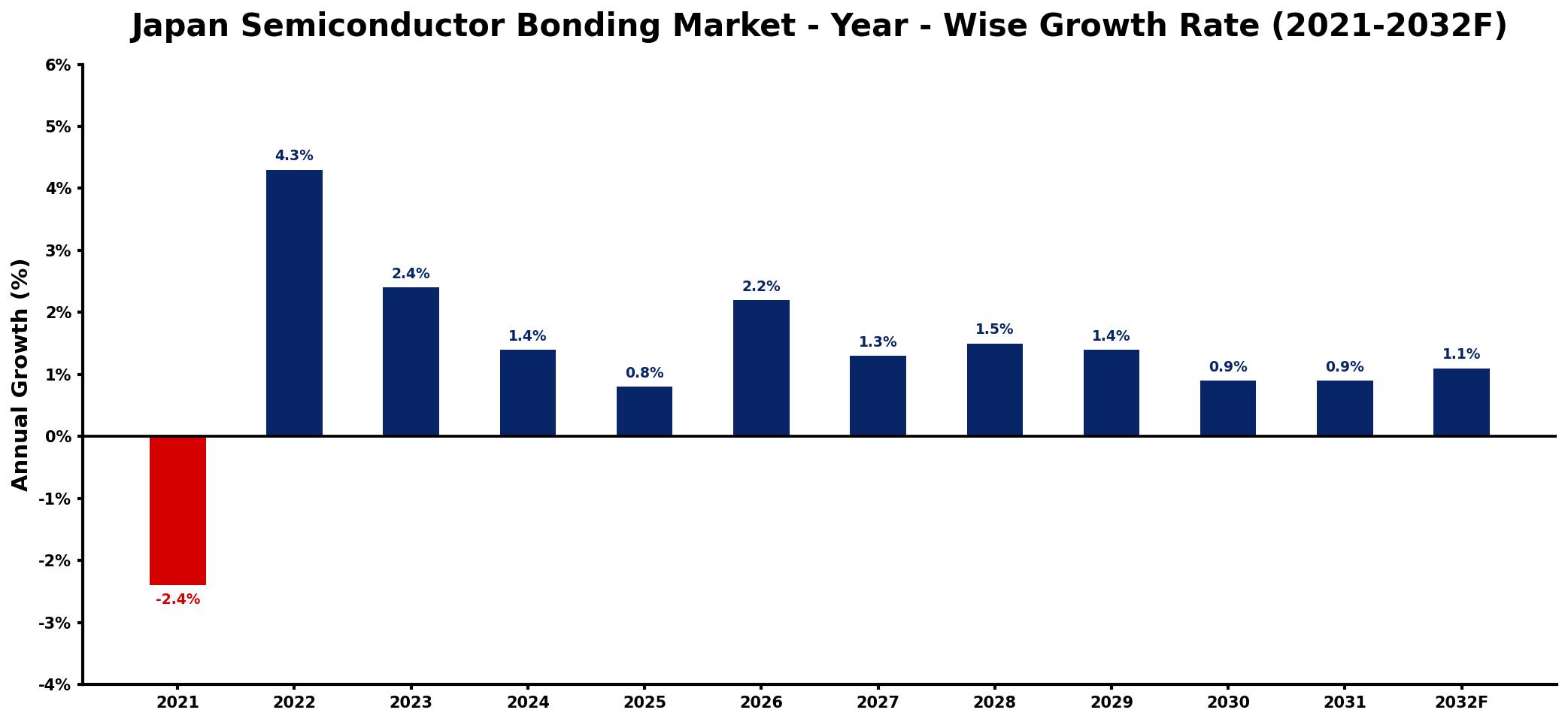
The table below presents the year‑wise growth rates along with the key drivers influencing the market
| Year | Growth Rate | Major Drivers |
| 2021 | -2.4% | Decreased investment in technology sector |
| 2022 | 4.3% | Rising demand for electronics manufacturing |
| 2023 | 2.4% | Expansion of automotive electronics market |
| 2024 | 1.4% | Increased focus on renewable energy |
| 2025 | 0.8% | Growth in consumer electronics sector |
| 2026 | 2.2% | Surge in telecommunications infrastructure projects |
| 2027 | 1.3% | Boost in IoT applications adoption |
| 2028 | 1.5% | Rising interest in smart devices |
| 2029 | 1.4% | increased overall sector activity |
| 2030 | 0.9% | growing regional consumption patterns |
| 2031 | 0.9% | Increase in data center expansions |
| 2032 | 1.1% | rising infrastructure development spending |
Note: Market size estimations and growth projections presented in this report are based on 6Wresearch's proprietary forecasting methodology, utilizing the latest available industry data, government publications, and primary research inputs.
Japan Semiconductor Bonding Market Synopsis
The Japan Semiconductor Bonding Market is characterized by significant technological advancements aimed at improving the performance and miniaturization of semiconductor devices. Wire bonding and flip chip bonding remain the dominant techniques, yet there is a notable shift towards innovative packaging solutions such as 3D IC stacking and system-in-package (SiP) technologies.
This market is buoyed by strong collaboration among semiconductor manufacturers and equipment suppliers, fostering a rich ecosystem for cutting-edge bonding solutions. The ability to effectively integrate heterogeneous materials is becoming increasingly important, especially in the context of emerging applications in sectors like automotive and healthcare.
Japan Semiconductor Bonding Market Key Takeaways
- The market is anticipated to evolve with advanced packaging solutions, driving demand for higher performance and reliability.
- Technological innovation remains a core focus, as companies invest heavily in R&D to enhance bonding capabilities.
- Strong partnerships between manufacturers and suppliers facilitate the availability of leading-edge bonding technologies.
- Sustainability concerns are prompting the development of eco-friendly bonding materials and processes.
- Intensifying global competition is pushing Japanese companies to innovate continuously to maintain market share.
Evaluation of Restraints in Japan Semiconductor Bonding Market
Despite its robust growth prospects, the Japan Semiconductor Bonding Market faces several constraints. The increasing complexity and miniaturization of semiconductor devices necessitate advanced bonding techniques, which heightens the demand for precision and reliability. This, in turn, leads to increased research and development costs. Furthermore, the call for environmentally friendly bonding materials poses additional challenges as manufacturers navigate compliance with stringent sustainability regulations. The competitive landscape is intense, with both established players and newcomers exerting pressure on pricing and innovation. External factors such as fluctuations in global demand and potential supply chain disruptions also add to the complexities faced by market participants.
Japan Semiconductor Bonding Market Trends
A notable trend in the Japan Semiconductor Bonding Market is the rising adoption of advanced packaging technologies, including fan-out wafer-level packaging (FOWLP) and 3D integration. These technologies provide enhanced performance, increased functionality, and improved reliability compared to traditional methods. Additionally, the market is leaning towards semiconductor bonding solutions that enable heterogeneous integration, a critical requirement for upcoming applications in sectors like artificial intelligence and healthcare. The focus on sustainable practices is also influencing material choices, prompting the development of more eco-friendly bonding processes.
Japan Semiconductor Bonding Market Opportunities
The Japan Semiconductor Bonding Market presents numerous investment opportunities, particularly as Japan continues to maintain a significant presence in the global semiconductor landscape. Companies engaged in bonding processes and equipment stand to benefit from the rising demand for advanced semiconductor devices. Furthermore, there is an opportunity for businesses to capitalize on the country's commitment to innovation, particularly in the realm of cutting-edge bonding technologies. As industries like automotive, consumer electronics, and healthcare increasingly require high-performance, miniaturized solutions, investors can find promising prospects in this evolving market.
Government Initiatives in the Japan Semiconductor Bonding Market
The Japanese government has introduced various initiatives to bolster the Semiconductor Bonding Market, aiming to reinforce the nation's stature in the global semiconductor industry. These initiatives include financial incentives for R&D activities, promoting collaboration between industry and academia, and fostering innovation across the sector. Sustainability is a key focus, with policies designed to encourage the adoption of eco-friendly practices and technologies within semiconductor manufacturing. Overall, these governmental strategies aim to create a conducive environment for growth and development in the Japan Semiconductor Bonding Market.
Future Insights of the Japan Semiconductor Bonding Market
Looking ahead to 2026-2032, the Japan Semiconductor Bonding Market is poised for steady growth driven by the escalating demand for advanced electronic devices across multiple industries. With technological advancements set to enhance bonding techniques, the market is likely to experience improved performance metrics and increased miniaturization. The proliferation of 5G technology, the Internet of Things (IoT), and artificial intelligence (AI) are expected to further catalyze demand for advanced semiconductor bonding solutions, underlining a positive outlook for this market segment.
Japan Semiconductor Bonding Market Latest Developments (2025 - 2026)
In the period leading up to June 2026, the Japan Semiconductor Bonding Market has seen notable movements toward enhanced collaboration among industry stakeholders. There is a growing emphasis on integrating advanced packaging solutions into existing semiconductor manufacturing processes. Additionally, several initiatives aimed at promoting sustainability within bonding technologies have gained traction, reflecting a broader industry trend toward eco-friendly practices. These developments indicate an ongoing commitment to innovation and responsiveness to market demands.
Japan Semiconductor Bonding Market - Key Attractiveness of the Report
- 10 Years of Market Numbers
- Historical Data Starting from 2022 to 2025
- Base Year: 2025
- Forecast Data until 2032
- Key Performance Indicators Impacting the Market
- Major Upcoming Developments and Projects
Key Highlights of the Report:
- Japan Semiconductor Bonding Market Outlook
- Market Size of Japan Semiconductor Bonding Market, 2025
- Forecast of Japan Semiconductor Bonding Market, 2032
- Historical Data and Forecast of Japan Semiconductor Bonding Revenues & Volume for the Period 2022-2032F
- Japan Semiconductor Bonding Market Trend Evolution
- Japan Semiconductor Bonding Market Drivers and Challenges
- Japan Semiconductor Bonding Price Trends
- Japan Semiconductor Bonding Porter's Five Forces
- Japan Semiconductor Bonding Industry Life Cycle
- Historical Data and Forecast of Japan Semiconductor Bonding Market Revenues & Volume By Type for the Period 2022-2032F
- Historical Data and Forecast of Japan Semiconductor Bonding Market Revenues & Volume By Die Bonder for the Period 2022-2032F
- Historical Data and Forecast of Japan Semiconductor Bonding Market Revenues & Volume By Wafer Bonder for the Period 2022-2032F
- Historical Data and Forecast of Japan Semiconductor Bonding Market Revenues & Volume By Flip Chip Bonder for the Period 2022-2032F
- Historical Data and Forecast of Japan Semiconductor Bonding Market Revenues & Volume By Proces Type for the Period 2022-2032F
- Historical Data and Forecast of Japan Semiconductor Bonding Market Revenues & Volume By Die-To-Die Bonding for the Period 2022-2032F
- Historical Data and Forecast of Japan Semiconductor Bonding Market Revenues & Volume By Die-To Wafer Bonding for the Period 2022-2032F
- Historical Data and Forecast of Japan Semiconductor Bonding Market Revenues & Volume By Wafer-To-Wafer Bonding for the Period 2022-2032F
- Historical Data and Forecast of Japan Semiconductor Bonding Market Revenues & Volume By Technology for the Period 2022-2032F
- Historical Data and Forecast of Japan Semiconductor Bonding Market Revenues & Volume By Direct Wafer Bonding for the Period 2022-2032F
- Historical Data and Forecast of Japan Semiconductor Bonding Market Revenues & Volume By Anodic Wafer Bonding for the Period 2022-2032F
- Historical Data and Forecast of Japan Semiconductor Bonding Market Revenues & Volume By Tcb Wafer Bonding for the Period 2022-2032F
- Historical Data and Forecast of Japan Semiconductor Bonding Market Revenues & Volume By Hybrid Bonding for the Period 2022-2032F
- Historical Data and Forecast of Japan Semiconductor Bonding Market Revenues & Volume By Others for the Period 2022-2032F
- Historical Data and Forecast of Japan Semiconductor Bonding Market Revenues & Volume By Application for the Period 2022-2032F
- Historical Data and Forecast of Japan Semiconductor Bonding Market Revenues & Volume By RF Devices for the Period 2022-2032F
- Historical Data and Forecast of Japan Semiconductor Bonding Market Revenues & Volume By Mems And Sensors for the Period 2022-2032F
- Historical Data and Forecast of Japan Semiconductor Bonding Market Revenues & Volume By Cmos Image Sensors for the Period 2022-2032F
- Historical Data and Forecast of Japan Semiconductor Bonding Market Revenues & Volume By LED for the Period 2022-2032F
- Historical Data and Forecast of Japan Semiconductor Bonding Market Revenues & Volume By 3D NAND for the Period 2022-2032F
- Japan Semiconductor Bonding Import Export Trade Statistics
- Market Opportunity Assessment By Type
- Market Opportunity Assessment By Proces Type
- Market Opportunity Assessment By Technology
- Market Opportunity Assessment By Application
- Japan Semiconductor Bonding Top Companies Market Share
- Japan Semiconductor Bonding Competitive Benchmarking By Technical and Operational Parameters
- Japan Semiconductor Bonding Company Profiles
- Japan Semiconductor Bonding Key Strategic Recommendations
Frequently Asked Questions About the Market Study (FAQs):
The market is estimated at USD 200 Million in 2025 and is projected to grow to USD 216 Million by 2032, reflecting a steady CAGR of 1.1% during the 2026-2032 period.
The automotive, consumer electronics, and industrial sectors are key drivers, as these industries increasingly require high-performance and miniaturized semiconductor devices.
Advanced packaging technologies such as 3D IC stacking and fan-out wafer-level packaging are gaining traction, offering better performance and reliability compared to traditional methods, thus reshaping market dynamics.
Manufacturers are contending with rising R&D costs due to the complexity and miniaturization of devices, as well as the need for sustainable bonding materials to comply with evolving regulations.
The Japanese government is actively promoting R&D and sustainability initiatives within the semiconductor industry, providing financial incentives and fostering collaboration to strengthen the market landscape.
Absolutely, the ongoing demand for advanced semiconductor devices presents significant growth and investment opportunities, particularly in companies focused on innovative bonding technologies.
6Wresearch actively monitors the Japan Semiconductor Bonding Market and publishes its comprehensive annual report, highlighting emerging trends, growth drivers, revenue analysis, and forecast outlook. Our insights help businesses to make data-backed strategic decisions with ongoing market dynamics. Our analysts track relevent industries related to the Japan Semiconductor Bonding Market, allowing our clients with actionable intelligence and reliable forecasts tailored to emerging regional needs.
Yes, we provide customisation as per your requirements. To learn more, feel free to contact us on sales@6wresearch.com
1 Executive Summary |
2 Introduction |
2.1 Key Highlights of the Report |
2.2 Report Description |
2.3 Market Scope & Segmentation |
2.4 Research Methodology |
2.5 Assumptions |
3 Japan Semiconductor Bonding Market Overview |
3.1 Japan Country Macro Economic Indicators |
3.2 Japan Semiconductor Bonding Market Revenues & Volume, 2022 & 2032F |
3.3 Japan Semiconductor Bonding Market - Industry Life Cycle |
3.4 Japan Semiconductor Bonding Market - Porter's Five Forces |
3.5 Japan Semiconductor Bonding Market Revenues & Volume Share, By Type, 2022 & 2032F |
3.6 Japan Semiconductor Bonding Market Revenues & Volume Share, By Proces Type, 2022 & 2032F |
3.7 Japan Semiconductor Bonding Market Revenues & Volume Share, By Technology, 2022 & 2032F |
3.8 Japan Semiconductor Bonding Market Revenues & Volume Share, By Application, 2022 & 2032F |
4 Japan Semiconductor Bonding Market Dynamics |
4.1 Impact Analysis |
4.2 Market Drivers |
4.2.1 Technological advancements in semiconductor bonding techniques |
4.2.2 Increasing demand for miniaturized electronic devices |
4.2.3 Growth in the automotive and consumer electronics industries in Japan |
4.3 Market Restraints |
4.3.1 High initial investment and operational costs associated with semiconductor bonding equipment |
4.3.2 Lack of skilled labor in the semiconductor industry in Japan |
5 Japan Semiconductor Bonding Market Trends |
6 Japan Semiconductor Bonding Market, By Types |
6.1 Japan Semiconductor Bonding Market, By Type |
6.1.1 Overview and Analysis |
6.1.2 Japan Semiconductor Bonding Market Revenues & Volume, By Type, 2022-2032F |
6.1.3 Japan Semiconductor Bonding Market Revenues & Volume, By Die Bonder, 2022-2032F |
6.1.4 Japan Semiconductor Bonding Market Revenues & Volume, By Wafer Bonder, 2022-2032F |
6.1.5 Japan Semiconductor Bonding Market Revenues & Volume, By Flip Chip Bonder, 2022-2032F |
6.2 Japan Semiconductor Bonding Market, By Proces Type |
6.2.1 Overview and Analysis |
6.2.2 Japan Semiconductor Bonding Market Revenues & Volume, By Die-To-Die Bonding, 2022-2032F |
6.2.3 Japan Semiconductor Bonding Market Revenues & Volume, By Die-To Wafer Bonding, 2022-2032F |
6.2.4 Japan Semiconductor Bonding Market Revenues & Volume, By Wafer-To-Wafer Bonding, 2022-2032F |
6.3 Japan Semiconductor Bonding Market, By Technology |
6.3.1 Overview and Analysis |
6.3.2 Japan Semiconductor Bonding Market Revenues & Volume, By Direct Wafer Bonding, 2022-2032F |
6.3.3 Japan Semiconductor Bonding Market Revenues & Volume, By Anodic Wafer Bonding, 2022-2032F |
6.3.4 Japan Semiconductor Bonding Market Revenues & Volume, By Tcb Wafer Bonding, 2022-2032F |
6.3.5 Japan Semiconductor Bonding Market Revenues & Volume, By Hybrid Bonding, 2022-2032F |
6.3.6 Japan Semiconductor Bonding Market Revenues & Volume, By Others, 2022-2032F |
6.4 Japan Semiconductor Bonding Market, By Application |
6.4.1 Overview and Analysis |
6.4.2 Japan Semiconductor Bonding Market Revenues & Volume, By RF Devices, 2022-2032F |
6.4.3 Japan Semiconductor Bonding Market Revenues & Volume, By Mems And Sensors, 2022-2032F |
6.4.4 Japan Semiconductor Bonding Market Revenues & Volume, By Cmos Image Sensors, 2022-2032F |
6.4.5 Japan Semiconductor Bonding Market Revenues & Volume, By LED, 2022-2032F |
6.4.6 Japan Semiconductor Bonding Market Revenues & Volume, By 3D NAND, 2022-2032F |
7 Japan Semiconductor Bonding Market Import-Export Trade Statistics |
7.1 Japan Semiconductor Bonding Market Export to Major Countries |
7.2 Japan Semiconductor Bonding Market Imports from Major Countries |
8 Japan Semiconductor Bonding Market Key Performance Indicators |
8.1 Percentage increase in research and development investments in semiconductor bonding technologies |
8.2 Number of patents filed for new semiconductor bonding techniques |
8.3 Adoption rate of advanced semiconductor bonding solutions in key industries such as automotive and consumer electronics |
9 Japan Semiconductor Bonding Market - Opportunity Assessment |
9.1 Japan Semiconductor Bonding Market Opportunity Assessment, By Type, 2022 & 2032F |
9.2 Japan Semiconductor Bonding Market Opportunity Assessment, By Proces Type, 2022 & 2032F |
9.3 Japan Semiconductor Bonding Market Opportunity Assessment, By Technology, 2022 & 2032F |
9.4 Japan Semiconductor Bonding Market Opportunity Assessment, By Application, 2022 & 2032F |
10 Japan Semiconductor Bonding Market - Competitive Landscape |
10.1 Japan Semiconductor Bonding Market Revenue Share, By Companies, 2025 |
10.2 Japan Semiconductor Bonding Market Competitive Benchmarking, By Operating and Technical Parameters |
11 Company Profiles |
12 Recommendations |
13 Disclaimer |
Global Go To Market Strategy - 2030
Export potential enables firms to identify high-growth global markets with greater confidence by combining advanced trade intelligence with a structured quantitative methodology. The framework analyzes emerging demand trends and country-level import patterns while integrating macroeconomic and trade datasets such as GDP and population forecasts, bilateral import–export flows, tariff structures, elasticity differentials between developed and developing economies, geographic distance, and import demand projections. Using weighted trade values from 2020–2024 as the base period to project country-to-country export potential for 2030, these inputs are operationalized through calculated drivers such as gravity model parameters, tariff impact factors, and projected GDP per-capita growth. Through an analysis of hidden potentials, demand hotspots, and market conditions that are most favorable to success, this method enables firms to focus on target countries, maximize returns, and global expansion with data, backed by accuracy.
By factoring in the projected importer demand gap that is currently unmet and could be potential opportunity, it identifies the potential for the Exporter (Country) among 190 countries, against the general trade analysis, which identifies the biggest importer or exporter.
To discover high-growth global markets and optimize your business strategy:
Click Here
Pricing
- Single User License$ 1,995
- Department License$ 2,400
- Site License$ 3,120
- Global License$ 3,795

Leadership Perspectives from Industry Events
Search
Thought Leadership and Analyst Meet


Our Clients
6WResearch In News
- India Export Attractiveness Tracker 2026
- India Air Conditioner Market Set for Strong Rebound in 2026 After Weather-Led Correction and GST-Driven Recovery: 6Wresearch
- ADAS in India: How Automatic Emergency Braking, Blind Spot Detection & Driver Monitoring are Transforming Road Safety
- Doha a strategic location for EV manufacturing hub: IPA Qatar
- Demand for luxury TVs surging in the GCC, says Samsung
- Empowering Growth: The Thriving Journey of Bangladesh’s Cable Industry
Latest Reports
- Nicaragua RPG Gaming Market (2026-2032)
- New Zealand RPG Gaming Market (2026-2032)
- Netherlands RPG Gaming Market (2026-2032)
- Nauru RPG Gaming Market (2026-2032)
- Namibia RPG Gaming Market (2026-2032)
- Mozambique RPG Gaming Market (2026-2032)
- Montenegro RPG Gaming Market (2026-2032)
- Mongolia RPG Gaming Market (2026-2032)
- Monaco RPG Gaming Market (2026-2032)
- Micronesia RPG Gaming Market (2026-2032)
Industry Events and Analyst Meet

EV India Expo 2026

HIMTEX 2026

India Refining Summit 2026

India EV Show 2026

EV tech India Expo 2026
Whitepaper
- Middle East & Africa Commercial Security Market Click here to view more.
- Middle East & Africa Fire Safety Systems & Equipment Market Click here to view more.
- GCC Drone Market Click here to view more.
- Middle East Lighting Fixture Market Click here to view more.
- GCC Physical & Perimeter Security Market Click here to view more.