Germany Semiconductor Metrology and Inspection Market (2026-2032) | Challenges, Value, Analysis, Competition, Consumer Insights, Demand, Competitive, Drivers, Industry, Strategic Insights, Outlook, Companies, Supply, Segmentation, Size, Segments, Growth, Trends, Share, Opportunities, Pricing Analysis, Revenue, Restraints, Investment Trends, Strategy, Forecast
Market Forecast By Type (Optical Metrology, Electron Microscopy, X-ray Metrology, AFM-Based Metrology), By Application (Wafer Inspection, Defect Inspection, Contamination Analysis, Packaging Inspection), By Equipment Type (Overlay Metrology, Critical Dimension Metrology, Metrology Software, Thin-Film Metrology), By Technology (2D Imaging, 3D Imaging, AI-Based, Spectroscopy), By Measurement Type (Surface Roughness, Film Thickness, Pattern Recognition, Dimensional Analysis) And Competitive Landscape
| Product Code: ETC11008011 | Publication Date: Apr 2025 | Updated Date: Mar 2026 | Product Type: Market Research Report | |
| Publisher: 6Wresearch | Author: Shubham Deep | No. of Pages: 65 | No. of Figures: 34 | No. of Tables: 19 |
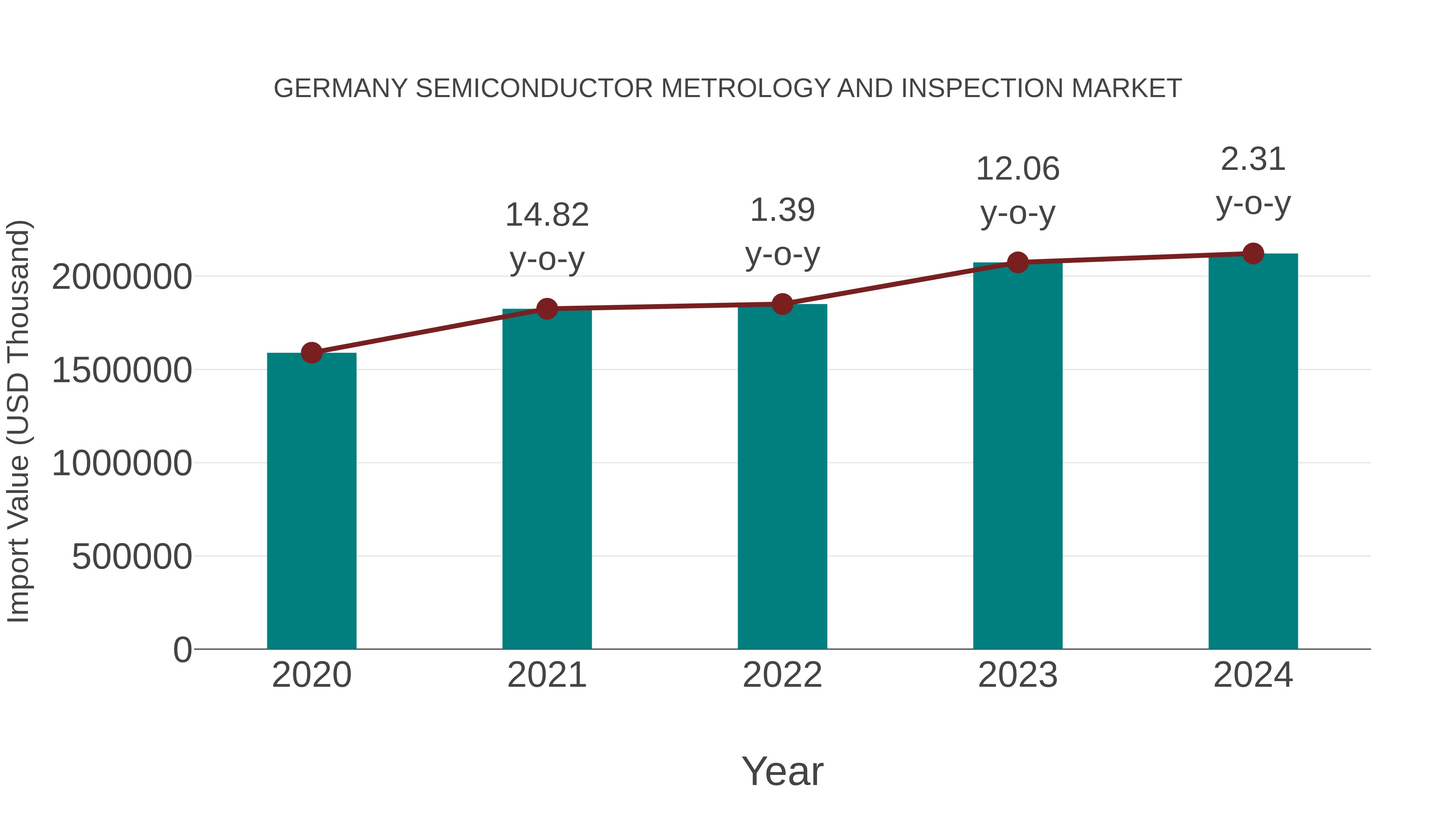
Germany Semiconductor Metrology and Inspection Market: Import Trend Analysis
Germany`s import trend for semiconductor metrology and inspection equipment showed a growth rate of 2.31% from 2023 to 2024, with a compound annual growth rate (CAGR) of 7.49% for the period 2020-2024. This growth can be attributed to the increasing demand for advanced technology in the semiconductor industry, driving the need for high-quality metrology and inspection equipment to ensure product quality and efficiency.
Germany Semiconductor Metrology and Inspection Market Overview
The semiconductor metrology and inspection market in Germany is experiencing steady growth driven by increasing demand for advanced semiconductor manufacturing processes. Key players in the market are focusing on developing innovative metrology and inspection technologies to enhance the quality and efficiency of semiconductor production. The market is characterized by the presence of leading companies such as Carl Zeiss AG, Infineon Technologies AG, and Applied Materials GmbH. Factors such as the growing adoption of IoT devices, autonomous vehicles, and artificial intelligence are fueling the demand for semiconductor metrology and inspection solutions. Additionally, government initiatives to promote digitalization and Industry 4.0 are further boosting market growth. Overall, the Germany semiconductor metrology and inspection market is expected to continue its positive trajectory in the coming years.
Germany Semiconductor Metrology and Inspection Market Trends
The Germany semiconductor metrology and inspection market is currently experiencing a shift towards more advanced and precise technologies to meet the increasing demands for quality control in semiconductor manufacturing. Key trends include the adoption of AI and machine learning for defect detection and analysis, the integration of multiple metrology techniques for comprehensive characterization, and the development of in-line inspection solutions to improve production efficiency. Additionally, there is a growing focus on sustainability and environmental impact, driving the demand for metrology tools that reduce energy consumption and waste generation. Overall, the market is witnessing rapid innovation and collaboration between semiconductor manufacturers and metrology equipment suppliers to address the evolving needs of the industry.
Germany Semiconductor Metrology and Inspection Market Challenges
In the Germany semiconductor metrology and inspection market, key challenges include the rapid technological advancements leading to the need for more precise and advanced metrology tools, the increasing complexity of semiconductor structures requiring higher resolution inspection capabilities, and the growing demand for faster and more accurate measurement techniques. Additionally, the market faces challenges related to high capital costs associated with acquiring state-of-the-art metrology and inspection equipment, as well as the need for skilled personnel to operate and interpret the data from these advanced tools. Moreover, increasing regulatory requirements and standards for semiconductor manufacturing processes further add to the challenges faced by companies operating in this market, necessitating continuous innovation and investment in research and development to stay competitive.
Germany Semiconductor Metrology and Inspection Market Investment Opportunities
The Germany semiconductor metrology and inspection market present promising investment opportunities due to the country`s strong presence in the semiconductor industry. With Germany being a hub for technological innovation and manufacturing, companies specializing in advanced metrology and inspection solutions for semiconductor production processes are in high demand. Investing in companies developing cutting-edge metrology tools, inspection equipment, and software solutions tailored to the specific needs of the German semiconductor market could yield significant returns. Additionally, with the increasing complexity and miniaturization of semiconductor devices, there is a growing need for high-precision metrology and inspection technologies, making this market segment particularly attractive for investors looking for long-term growth potential in the semiconductor industry.
Germany Semiconductor Metrology and Inspection Market Government Policy
The German government has implemented various policies to support the semiconductor metrology and inspection market, aiming to strengthen the country`s position in the global semiconductor industry. These policies include investment in research and development initiatives to drive innovation in metrology technologies, as well as incentives for companies to expand their semiconductor manufacturing capabilities in Germany. Additionally, the government has established partnerships with industry stakeholders and research institutions to promote collaboration and knowledge-sharing in advancing metrology and inspection solutions. Furthermore, there is a focus on fostering a skilled workforce through education and training programs to meet the growing demands of the semiconductor sector. Overall, these policies demonstrate a commitment to enhancing the competitiveness and sustainability of the semiconductor metrology and inspection market in Germany.
Germany Semiconductor Metrology and Inspection Market Future Outlook
The future outlook for the Germany semiconductor metrology and inspection market is expected to be positive, driven by technological advancements in the semiconductor industry and increasing demand for high-quality and reliable semiconductor products. The market is likely to witness growth due to the rising adoption of advanced metrology and inspection tools for ensuring quality control and process optimization in semiconductor manufacturing. Additionally, the increasing focus on research and development activities to enhance semiconductor production processes and improve product performance is anticipated to further propel market growth. With Germany being a key player in the global semiconductor industry, the country`s strong infrastructure, skilled workforce, and commitment to innovation are poised to contribute to the expansion of the semiconductor metrology and inspection market in the region.
Key Highlights of the Report:
- Germany Semiconductor Metrology and Inspection Market Outlook
- Market Size of Germany Semiconductor Metrology and Inspection Market,2025
- Forecast of Germany Semiconductor Metrology and Inspection Market, 2032
- Historical Data and Forecast of Germany Semiconductor Metrology and Inspection Revenues & Volume for the Period 2022-2032F
- Germany Semiconductor Metrology and Inspection Market Trend Evolution
- Germany Semiconductor Metrology and Inspection Market Drivers and Challenges
- Germany Semiconductor Metrology and Inspection Price Trends
- Germany Semiconductor Metrology and Inspection Porter's Five Forces
- Germany Semiconductor Metrology and Inspection Industry Life Cycle
- Historical Data and Forecast of Germany Semiconductor Metrology and Inspection Market Revenues & Volume By Type for the Period 2022-2032F
- Historical Data and Forecast of Germany Semiconductor Metrology and Inspection Market Revenues & Volume By Optical Metrology for the Period 2022-2032F
- Historical Data and Forecast of Germany Semiconductor Metrology and Inspection Market Revenues & Volume By Electron Microscopy for the Period 2022-2032F
- Historical Data and Forecast of Germany Semiconductor Metrology and Inspection Market Revenues & Volume By X-ray Metrology for the Period 2022-2032F
- Historical Data and Forecast of Germany Semiconductor Metrology and Inspection Market Revenues & Volume By AFM-Based Metrology for the Period 2022-2032F
- Historical Data and Forecast of Germany Semiconductor Metrology and Inspection Market Revenues & Volume By Application for the Period 2022-2032F
- Historical Data and Forecast of Germany Semiconductor Metrology and Inspection Market Revenues & Volume By Wafer Inspection for the Period 2022-2032F
- Historical Data and Forecast of Germany Semiconductor Metrology and Inspection Market Revenues & Volume By Defect Inspection for the Period 2022-2032F
- Historical Data and Forecast of Germany Semiconductor Metrology and Inspection Market Revenues & Volume By Contamination Analysis for the Period 2022-2032F
- Historical Data and Forecast of Germany Semiconductor Metrology and Inspection Market Revenues & Volume By Packaging Inspection for the Period 2022-2032F
- Historical Data and Forecast of Germany Semiconductor Metrology and Inspection Market Revenues & Volume By Equipment Type for the Period 2022-2032F
- Historical Data and Forecast of Germany Semiconductor Metrology and Inspection Market Revenues & Volume By Overlay Metrology for the Period 2022-2032F
- Historical Data and Forecast of Germany Semiconductor Metrology and Inspection Market Revenues & Volume By Critical Dimension Metrology for the Period 2022-2032F
- Historical Data and Forecast of Germany Semiconductor Metrology and Inspection Market Revenues & Volume By Metrology Software for the Period 2022-2032F
- Historical Data and Forecast of Germany Semiconductor Metrology and Inspection Market Revenues & Volume By Thin-Film Metrology for the Period 2022-2032F
- Historical Data and Forecast of Germany Semiconductor Metrology and Inspection Market Revenues & Volume By Technology for the Period 2022-2032F
- Historical Data and Forecast of Germany Semiconductor Metrology and Inspection Market Revenues & Volume By 2D Imaging for the Period 2022-2032F
- Historical Data and Forecast of Germany Semiconductor Metrology and Inspection Market Revenues & Volume By 3D Imaging for the Period 2022-2032F
- Historical Data and Forecast of Germany Semiconductor Metrology and Inspection Market Revenues & Volume By AI-Based for the Period 2022-2032F
- Historical Data and Forecast of Germany Semiconductor Metrology and Inspection Market Revenues & Volume By Spectroscopy for the Period 2022-2032F
- Historical Data and Forecast of Germany Semiconductor Metrology and Inspection Market Revenues & Volume By Measurement Type for the Period 2022-2032F
- Historical Data and Forecast of Germany Semiconductor Metrology and Inspection Market Revenues & Volume By Surface Roughness for the Period 2022-2032F
- Historical Data and Forecast of Germany Semiconductor Metrology and Inspection Market Revenues & Volume By Film Thickness for the Period 2022-2032F
- Historical Data and Forecast of Germany Semiconductor Metrology and Inspection Market Revenues & Volume By Pattern Recognition for the Period 2022-2032F
- Historical Data and Forecast of Germany Semiconductor Metrology and Inspection Market Revenues & Volume By Dimensional Analysis for the Period 2022-2032F
- Germany Semiconductor Metrology and Inspection Import Export Trade Statistics
- Market Opportunity Assessment By Type
- Market Opportunity Assessment By Application
- Market Opportunity Assessment By Equipment Type
- Market Opportunity Assessment By Technology
- Market Opportunity Assessment By Measurement Type
- Germany Semiconductor Metrology and Inspection Top Companies Market Share
- Germany Semiconductor Metrology and Inspection Competitive Benchmarking By Technical and Operational Parameters
- Germany Semiconductor Metrology and Inspection Company Profiles
- Germany Semiconductor Metrology and Inspection Key Strategic Recommendations
Germany Semiconductor Metrology and Inspection Market (2026-2032): FAQs
6Wresearch actively monitors the Germany Semiconductor Metrology and Inspection Market and publishes its comprehensive annual report, highlighting emerging trends, growth drivers, revenue analysis, and forecast outlook. Our insights help businesses to make data-backed strategic decisions with ongoing market dynamics. Our analysts track relevent industries related to the Germany Semiconductor Metrology and Inspection Market, allowing our clients with actionable intelligence and reliable forecasts tailored to emerging regional needs.
Yes, we provide customisation as per your requirements. To learn more, feel free to contact us on sales@6wresearch.com
1 Executive Summary |
2 Introduction |
2.1 Key Highlights of the Report |
2.2 Report Description |
2.3 Market Scope & Segmentation |
2.4 Research Methodology |
2.5 Assumptions |
3 Germany Semiconductor Metrology and Inspection Market Overview |
3.1 Germany Country Macro Economic Indicators |
3.2 Germany Semiconductor Metrology and Inspection Market Revenues & Volume, 2022 & 2032F |
3.3 Germany Semiconductor Metrology and Inspection Market - Industry Life Cycle |
3.4 Germany Semiconductor Metrology and Inspection Market - Porter's Five Forces |
3.5 Germany Semiconductor Metrology and Inspection Market Revenues & Volume Share, By Type, 2022 & 2032F |
3.6 Germany Semiconductor Metrology and Inspection Market Revenues & Volume Share, By Application, 2022 & 2032F |
3.7 Germany Semiconductor Metrology and Inspection Market Revenues & Volume Share, By Equipment Type, 2022 & 2032F |
3.8 Germany Semiconductor Metrology and Inspection Market Revenues & Volume Share, By Technology, 2022 & 2032F |
3.9 Germany Semiconductor Metrology and Inspection Market Revenues & Volume Share, By Measurement Type, 2022 & 2032F |
4 Germany Semiconductor Metrology and Inspection Market Dynamics |
4.1 Impact Analysis |
4.2 Market Drivers |
4.2.1 Technological advancements in semiconductor manufacturing |
4.2.2 Increasing demand for high-quality and reliable electronic devices |
4.2.3 Growing focus on quality control and assurance in semiconductor production |
4.3 Market Restraints |
4.3.1 High initial investment and operational costs associated with semiconductor metrology and inspection equipment |
4.3.2 Lack of skilled workforce in the field of semiconductor metrology and inspection |
5 Germany Semiconductor Metrology and Inspection Market Trends |
6 Germany Semiconductor Metrology and Inspection Market, By Types |
6.1 Germany Semiconductor Metrology and Inspection Market, By Type |
6.1.1 Overview and Analysis |
6.1.2 Germany Semiconductor Metrology and Inspection Market Revenues & Volume, By Type, 2022-2032F |
6.1.3 Germany Semiconductor Metrology and Inspection Market Revenues & Volume, By Optical Metrology, 2022-2032F |
6.1.4 Germany Semiconductor Metrology and Inspection Market Revenues & Volume, By Electron Microscopy, 2022-2032F |
6.1.5 Germany Semiconductor Metrology and Inspection Market Revenues & Volume, By X-ray Metrology, 2022-2032F |
6.1.6 Germany Semiconductor Metrology and Inspection Market Revenues & Volume, By AFM-Based Metrology, 2022-2032F |
6.2 Germany Semiconductor Metrology and Inspection Market, By Application |
6.2.1 Overview and Analysis |
6.2.2 Germany Semiconductor Metrology and Inspection Market Revenues & Volume, By Wafer Inspection, 2022-2032F |
6.2.3 Germany Semiconductor Metrology and Inspection Market Revenues & Volume, By Defect Inspection, 2022-2032F |
6.2.4 Germany Semiconductor Metrology and Inspection Market Revenues & Volume, By Contamination Analysis, 2022-2032F |
6.2.5 Germany Semiconductor Metrology and Inspection Market Revenues & Volume, By Packaging Inspection, 2022-2032F |
6.3 Germany Semiconductor Metrology and Inspection Market, By Equipment Type |
6.3.1 Overview and Analysis |
6.3.2 Germany Semiconductor Metrology and Inspection Market Revenues & Volume, By Overlay Metrology, 2022-2032F |
6.3.3 Germany Semiconductor Metrology and Inspection Market Revenues & Volume, By Critical Dimension Metrology, 2022-2032F |
6.3.4 Germany Semiconductor Metrology and Inspection Market Revenues & Volume, By Metrology Software, 2022-2032F |
6.3.5 Germany Semiconductor Metrology and Inspection Market Revenues & Volume, By Thin-Film Metrology, 2022-2032F |
6.4 Germany Semiconductor Metrology and Inspection Market, By Technology |
6.4.1 Overview and Analysis |
6.4.2 Germany Semiconductor Metrology and Inspection Market Revenues & Volume, By 2D Imaging, 2022-2032F |
6.4.3 Germany Semiconductor Metrology and Inspection Market Revenues & Volume, By 3D Imaging, 2022-2032F |
6.4.4 Germany Semiconductor Metrology and Inspection Market Revenues & Volume, By AI-Based, 2022-2032F |
6.4.5 Germany Semiconductor Metrology and Inspection Market Revenues & Volume, By Spectroscopy, 2022-2032F |
6.5 Germany Semiconductor Metrology and Inspection Market, By Measurement Type |
6.5.1 Overview and Analysis |
6.5.2 Germany Semiconductor Metrology and Inspection Market Revenues & Volume, By Surface Roughness, 2022-2032F |
6.5.3 Germany Semiconductor Metrology and Inspection Market Revenues & Volume, By Film Thickness, 2022-2032F |
6.5.4 Germany Semiconductor Metrology and Inspection Market Revenues & Volume, By Pattern Recognition, 2022-2032F |
6.5.5 Germany Semiconductor Metrology and Inspection Market Revenues & Volume, By Dimensional Analysis, 2022-2032F |
7 Germany Semiconductor Metrology and Inspection Market Import-Export Trade Statistics |
7.1 Germany Semiconductor Metrology and Inspection Market Export to Major Countries |
7.2 Germany Semiconductor Metrology and Inspection Market Imports from Major Countries |
8 Germany Semiconductor Metrology and Inspection Market Key Performance Indicators |
8.1 Average equipment utilization rate |
8.2 Percentage of defects detected and resolved in semiconductor manufacturing processes |
8.3 Rate of adoption of advanced metrology and inspection technologies in the semiconductor industry |
9 Germany Semiconductor Metrology and Inspection Market - Opportunity Assessment |
9.1 Germany Semiconductor Metrology and Inspection Market Opportunity Assessment, By Type, 2022 & 2032F |
9.2 Germany Semiconductor Metrology and Inspection Market Opportunity Assessment, By Application, 2022 & 2032F |
9.3 Germany Semiconductor Metrology and Inspection Market Opportunity Assessment, By Equipment Type, 2022 & 2032F |
9.4 Germany Semiconductor Metrology and Inspection Market Opportunity Assessment, By Technology, 2022 & 2032F |
9.5 Germany Semiconductor Metrology and Inspection Market Opportunity Assessment, By Measurement Type, 2022 & 2032F |
10 Germany Semiconductor Metrology and Inspection Market - Competitive Landscape |
10.1 Germany Semiconductor Metrology and Inspection Market Revenue Share, By Companies, 2025 |
10.2 Germany Semiconductor Metrology and Inspection Market Competitive Benchmarking, By Operating and Technical Parameters |
11 Company Profiles |
12 Recommendations |
13 Disclaimer |
Export potential assessment - trade Analytics for 2030
Export potential enables firms to identify high-growth global markets with greater confidence by combining advanced trade intelligence with a structured quantitative methodology. The framework analyzes emerging demand trends and country-level import patterns while integrating macroeconomic and trade datasets such as GDP and population forecasts, bilateral import–export flows, tariff structures, elasticity differentials between developed and developing economies, geographic distance, and import demand projections. Using weighted trade values from 2020–2024 as the base period to project country-to-country export potential for 2030, these inputs are operationalized through calculated drivers such as gravity model parameters, tariff impact factors, and projected GDP per-capita growth. Through an analysis of hidden potentials, demand hotspots, and market conditions that are most favorable to success, this method enables firms to focus on target countries, maximize returns, and global expansion with data, backed by accuracy.
By factoring in the projected importer demand gap that is currently unmet and could be potential opportunity, it identifies the potential for the Exporter (Country) among 190 countries, against the general trade analysis, which identifies the biggest importer or exporter.
To discover high-growth global markets and optimize your business strategy:
Click Here
Pricing
- Single User License$ 1,995
- Department License$ 2,400
- Site License$ 3,120
- Global License$ 3,795

Search
Thought Leadership and Analyst Meet


Our Clients
Latest Reports
- Canada Cloud CFD Market (2026-2032) | Size & Revenue, Industry, Growth, Competitive Landscape, Forecast, Segmentation, Value, Outlook, Trends, Share, Analysis, Companies
- Taiwan Food Delivery Platform Market (2026-2032) | Companies, Outlook, Analysis, Trends, Value, Revenue, Segmentation, Share, Forecast, Competitive Landscape, Growth, Size & Forecast
- United Kingdom (UK) Long-term Care Insurance Market (2026-2032) | Growth, Share, Consumer Insights, Drivers, Opportunities, Competition, Pricing Analysis, Segments, Restraints, Companies, Competitive, Value, Outlook, Size, Demand, Analysis, Challenges, Strategic Insights, Investment Trends, Revenue, Trends, Supply, Forecast
- United Kingdom (UK) Long Term Care Market (2026-2032) | Companies, Outlook, Analysis, Trends, Value, Revenue, Segmentation, Share, Forecast, Competitive Landscape, Growth, Size & Forecast
- Iraq Insulation and Waterproofing Market (2026-2032) | Outlook, Drivers, Growth, Size, Share, Industry, Revenue, Trends, Demand, Competitive, Strategic Insights, Opportunities, Segments, Companies, Challenges, Strategy, Consumer Insights, Analysis, Investment Trends, Value, Segmentation, Forecast, Restraints
- India Switchgear Market Outlook (2026-2032) | Size, Share, Trends, Growth, Revenue, Forecast, Analysis, Value, Outlook
- Pakistan Contraceptive Implants Market (2025-2031) | Demand, Growth, Size, Share, Industry, Pricing Analysis, Competitive, Strategic Insights, Strategy, Consumer Insights, Analysis, Investment Trends, Opportunities, Revenue, Segments, Value, Segmentation, Supply, Forecast, Restraints, Outlook, Competition, Drivers, Trends, Companies, Challenges
- Sri Lanka Packaging Market (2026-2032) | Outlook, Competition, Drivers, Trends, Demand, Pricing Analysis, Competitive, Strategic Insights, Companies, Challenges, Strategy, Consumer Insights, Analysis, Investment Trends, Opportunities, Growth, Size, Share, Industry, Revenue, Segments, Value, Segmentation, Supply, Forecast, Restraints
- India Kids Watches Market (2026-2032) | Strategy, Consumer Insights, Analysis, Investment Trends, Opportunities, Growth, Size, Share, Industry, Revenue, Segments, Value, Segmentation, Supply, Forecast, Restraints, Outlook, Competition, Drivers, Trends, Demand, Pricing Analysis, Competitive, Strategic Insights, Companies, Challenges
- Saudi Arabia Core Assurance Service Market (2025-2031) | Strategy, Consumer Insights, Analysis, Investment Trends, Opportunities, Growth, Size, Share, Industry, Revenue, Segments, Value, Segmentation, Supply, Forecast, Restraints, Outlook, Competition, Drivers, Trends, Demand, Pricing Analysis, Competitive, Strategic Insights, Companies, Challenges
Industry Events and Analyst Meet

India EV Show 2026

EV tech India Expo 2026

Auto Tech Asia 2026

Battery Tech India 2026

Smart Production Solutions Guangzhou 2026
Whitepaper
- Middle East & Africa Commercial Security Market Click here to view more.
- Middle East & Africa Fire Safety Systems & Equipment Market Click here to view more.
- GCC Drone Market Click here to view more.
- Middle East Lighting Fixture Market Click here to view more.
- GCC Physical & Perimeter Security Market Click here to view more.
6WResearch In News
- Doha a strategic location for EV manufacturing hub: IPA Qatar
- Demand for luxury TVs surging in the GCC, says Samsung
- Empowering Growth: The Thriving Journey of Bangladesh’s Cable Industry
- Demand for luxury TVs surging in the GCC, says Samsung
- Video call with a traditional healer? Once unthinkable, it’s now common in South Africa
- Intelligent Buildings To Smooth GCC’s Path To Net Zero