Germany Semiconductor Bonding Market (2026-2032) Outlook | Revenue, Analysis, Growth, Size, Industry, Forecast, Companies, Value, Share, Trends
Market Forecast By Type (Die Bonder, Wafer Bonder, Flip Chip Bonder), By Proces Type (Die-To-Die Bonding, Die-To Wafer Bonding, Wafer-To-Wafer Bonding), By Technology (Direct Wafer Bonding, Anodic Wafer Bonding, Tcb Wafer Bonding, Hybrid Bonding, Others), By Application (RF Devices, Mems And Sensors, Cmos Image Sensors, LED, 3D NAND) And Competitive Landscape
| Product Code: ETC305051 | Publication Date: Aug 2022 | Updated Date: Mar 2026 | Product Type: Market Research Report | |
| Publisher: 6Wresearch | Author: Bhawna Singh | No. of Pages: 75 | No. of Figures: 35 | No. of Tables: 20 |
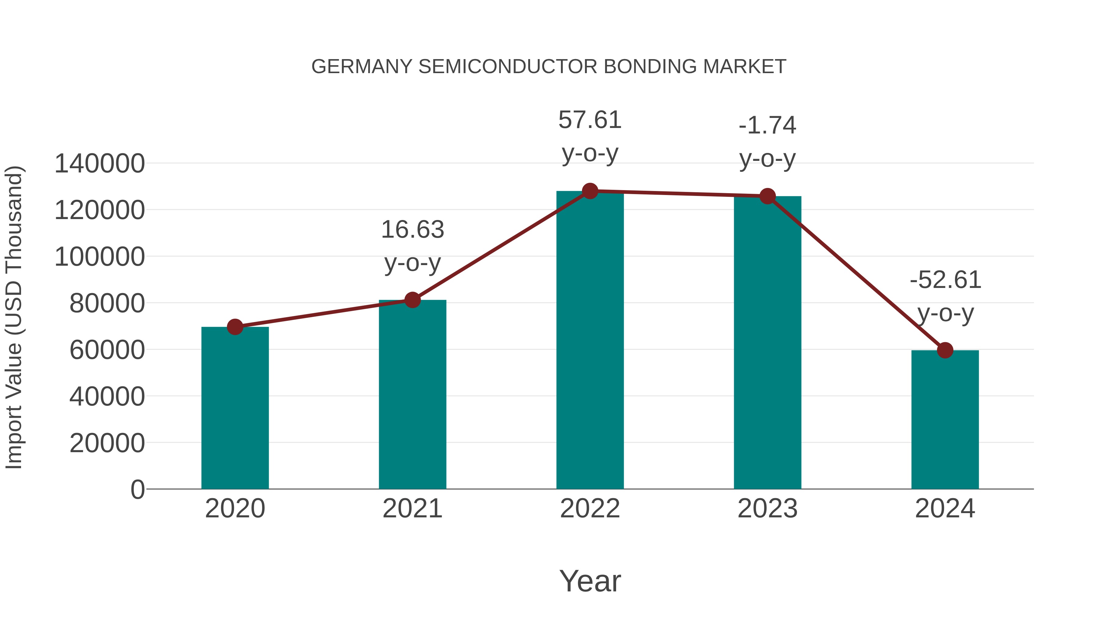
Germany Semiconductor Bonding Market: Import Trend Analysis
Germany`s import trend for the semiconductor bonding market experienced a significant decline from 2023 to 2024, with a growth rate of -52.61%. The compound annual growth rate (CAGR) from 2020 to 2024 stood at -3.81%. This substantial decrease in import momentum can be attributed to shifts in demand dynamics or potential market stabilization efforts.
Germany Semiconductor Bonding Market Synopsis
The Germany Semiconductor Bonding Market is a significant segment within the country`s electronics industry. With the presence of major semiconductor manufacturers and a strong focus on innovation and technology, Germany is a key player in the global semiconductor bonding market. The market is driven by the increasing demand for advanced semiconductor devices in various applications such as automotive, healthcare, and telecommunications. Key trends in the market include the adoption of advanced bonding technologies like copper wire bonding and the development of smaller, more efficient packages. Additionally, the market is influenced by factors such as government initiatives to promote the semiconductor industry and partnerships between local companies and international players. Overall, the Germany Semiconductor Bonding Market is poised for further growth and innovation in the coming years.
Germany Semiconductor Bonding Market Trends
In the Germany Semiconductor Bonding Market, there is a noticeable trend towards the adoption of advanced packaging technologies such as System-in-Package (SiP) and Wafer-Level Packaging (WLP). These technologies are gaining traction due to their ability to enhance performance, reduce form factor, and improve overall cost-efficiency in semiconductor devices. Additionally, there is a growing emphasis on the development of bonding processes that enable higher integration levels and improved reliability in electronic components. Key players in the market are investing in research and development efforts to innovate new bonding solutions that meet the evolving requirements of industries such as automotive, consumer electronics, and telecommunications. Overall, the Germany Semiconductor Bonding Market is witnessing a shift towards more sophisticated bonding techniques to meet the demands of increasingly complex semiconductor devices.
Germany Semiconductor Bonding Market Challenges
In the Germany Semiconductor Bonding Market, some of the key challenges faced include increasing complexity in semiconductor designs, demand for higher performance and miniaturization, and the need for advanced bonding technologies to meet these requirements. Additionally, there is a growing focus on environmental sustainability and regulations, which necessitate the development of eco-friendly bonding processes. Moreover, competition from other global semiconductor manufacturing hubs poses a challenge for German companies to stay competitive and innovative in the market. Adapting to rapidly evolving technologies and market trends, as well as addressing supply chain disruptions and geopolitical uncertainties, are also significant challenges faced by players in the Germany Semiconductor Bonding Market.
Germany Semiconductor Bonding Market Investment Opportunities
In the Germany Semiconductor Bonding Market, there are promising investment opportunities driven by the increasing demand for advanced semiconductor technologies across various industries such as automotive, electronics, and healthcare. With Germany being a key player in the European semiconductor industry, there is a growing need for innovative bonding solutions to enhance performance and efficiency in semiconductor devices. Investing in companies that specialize in semiconductor bonding equipment, materials, and services can be lucrative as they cater to the evolving needs of the market. Additionally, as the focus on renewable energy sources and electric vehicles grows, there is a rising demand for semiconductor bonding technologies to support these sectors, presenting further investment potential in this market segment.
Jordan Agar Market Government Policies
In Germany, the semiconductor bonding market is influenced by various government policies aimed at promoting innovation and technology development. The German government has been supportive of the semiconductor industry through initiatives such as funding for research and development, fostering collaboration between industry and academia, and providing incentives for companies to invest in manufacturing facilities. Additionally, there are regulations in place to ensure the quality and safety of semiconductor products, as well as to promote sustainability and environmental protection in the manufacturing process. Overall, the government`s policies in Germany create a conducive environment for the growth and competitiveness of the semiconductor bonding market by encouraging innovation, investment, and compliance with industry standards.
Germany Semiconductor Bonding Market Future Outlook
The Germany Semiconductor Bonding Market is poised for steady growth in the coming years, driven by increasing demand for advanced semiconductor devices across various industries such as automotive, electronics, and healthcare. The market is expected to benefit from technological advancements in semiconductor bonding techniques, such as the adoption of advanced materials and processes like copper wire bonding and high-density interconnects. Additionally, the rising trend of miniaturization and integration of components in electronic devices is likely to fuel the demand for semiconductor bonding solutions. With Germany being a key player in the global semiconductor industry, the market is anticipated to witness sustained growth, supported by investments in research and development activities to enhance semiconductor bonding technologies and meet the evolving needs of the market.
Key Highlights of the Report:
- Germany Semiconductor Bonding Market Outlook
- Market Size of Germany Semiconductor Bonding Market, 2025
- Forecast of Germany Semiconductor Bonding Market, 2032
- Historical Data and Forecast of Germany Semiconductor Bonding Revenues & Volume for the Period 2022 - 2032F
- Germany Semiconductor Bonding Market Trend Evolution
- Germany Semiconductor Bonding Market Drivers and Challenges
- Germany Semiconductor Bonding Price Trends
- Germany Semiconductor Bonding Porter's Five Forces
- Germany Semiconductor Bonding Industry Life Cycle
- Historical Data and Forecast of Germany Semiconductor Bonding Market Revenues & Volume By Type for the Period 2022 - 2032F
- Historical Data and Forecast of Germany Semiconductor Bonding Market Revenues & Volume By Die Bonder for the Period 2022 - 2032F
- Historical Data and Forecast of Germany Semiconductor Bonding Market Revenues & Volume By Wafer Bonder for the Period 2022 - 2032F
- Historical Data and Forecast of Germany Semiconductor Bonding Market Revenues & Volume By Flip Chip Bonder for the Period 2022 - 2032F
- Historical Data and Forecast of Germany Semiconductor Bonding Market Revenues & Volume By Proces Type for the Period 2022 - 2032F
- Historical Data and Forecast of Germany Semiconductor Bonding Market Revenues & Volume By Die-To-Die Bonding for the Period 2022 - 2032F
- Historical Data and Forecast of Germany Semiconductor Bonding Market Revenues & Volume By Die-To Wafer Bonding for the Period 2022 - 2032F
- Historical Data and Forecast of Germany Semiconductor Bonding Market Revenues & Volume By Wafer-To-Wafer Bonding for the Period 2022 - 2032F
- Historical Data and Forecast of Germany Semiconductor Bonding Market Revenues & Volume By Technology for the Period 2022 - 2032F
- Historical Data and Forecast of Germany Semiconductor Bonding Market Revenues & Volume By Direct Wafer Bonding for the Period 2022 - 2032F
- Historical Data and Forecast of Germany Semiconductor Bonding Market Revenues & Volume By Anodic Wafer Bonding for the Period 2022 - 2032F
- Historical Data and Forecast of Germany Semiconductor Bonding Market Revenues & Volume By Tcb Wafer Bonding for the Period 2022 - 2032F
- Historical Data and Forecast of Germany Semiconductor Bonding Market Revenues & Volume By Hybrid Bonding for the Period 2022 - 2032F
- Historical Data and Forecast of Germany Semiconductor Bonding Market Revenues & Volume By Others for the Period 2022 - 2032F
- Historical Data and Forecast of Germany Semiconductor Bonding Market Revenues & Volume By Application for the Period 2022 - 2032F
- Historical Data and Forecast of Germany Semiconductor Bonding Market Revenues & Volume By RF Devices for the Period 2022 - 2032F
- Historical Data and Forecast of Germany Semiconductor Bonding Market Revenues & Volume By Mems And Sensors for the Period 2022 - 2032F
- Historical Data and Forecast of Germany Semiconductor Bonding Market Revenues & Volume By Cmos Image Sensors for the Period 2022 - 2032F
- Historical Data and Forecast of Germany Semiconductor Bonding Market Revenues & Volume By LED for the Period 2022 - 2032F
- Historical Data and Forecast of Germany Semiconductor Bonding Market Revenues & Volume By 3D NAND for the Period 2022 - 2032F
- Germany Semiconductor Bonding Import Export Trade Statistics
- Market Opportunity Assessment By Type
- Market Opportunity Assessment By Proces Type
- Market Opportunity Assessment By Technology
- Market Opportunity Assessment By Application
- Germany Semiconductor Bonding Top Companies Market Share
- Germany Semiconductor Bonding Competitive Benchmarking By Technical and Operational Parameters
- Germany Semiconductor Bonding Company Profiles
- Germany Semiconductor Bonding Key Strategic Recommendations
Germany Semiconductor Bonding Market (2026-2032): FAQs
6Wresearch actively monitors the Germany Semiconductor Bonding Market and publishes its comprehensive annual report, highlighting emerging trends, growth drivers, revenue analysis, and forecast outlook. Our insights help businesses to make data-backed strategic decisions with ongoing market dynamics. Our analysts track relevent industries related to the Germany Semiconductor Bonding Market, allowing our clients with actionable intelligence and reliable forecasts tailored to emerging regional needs.
Yes, we provide customisation as per your requirements. To learn more, feel free to contact us on sales@6wresearch.com
1 Executive Summary |
2 Introduction |
2.1 Key Highlights of the Report |
2.2 Report Description |
2.3 Market Scope & Segmentation |
2.4 Research Methodology |
2.5 Assumptions |
3 Germany Semiconductor Bonding Market Overview |
3.1 Germany Country Macro Economic Indicators |
3.2 Germany Semiconductor Bonding Market Revenues & Volume, 2022 & 2032F |
3.3 Germany Semiconductor Bonding Market - Industry Life Cycle |
3.4 Germany Semiconductor Bonding Market - Porter's Five Forces |
3.5 Germany Semiconductor Bonding Market Revenues & Volume Share, By Type, 2022 & 2032F |
3.6 Germany Semiconductor Bonding Market Revenues & Volume Share, By Proces Type, 2022 & 2032F |
3.7 Germany Semiconductor Bonding Market Revenues & Volume Share, By Technology, 2022 & 2032F |
3.8 Germany Semiconductor Bonding Market Revenues & Volume Share, By Application, 2022 & 2032F |
4 Germany Semiconductor Bonding Market Dynamics |
4.1 Impact Analysis |
4.2 Market Drivers |
4.2.1 Technological advancements in semiconductor bonding techniques |
4.2.2 Increasing demand for compact electronic devices |
4.2.3 Growth in the automotive and industrial sectors in Germany |
4.3 Market Restraints |
4.3.1 High initial investment costs for semiconductor bonding equipment |
4.3.2 Stringent regulations and standards in the semiconductor industry |
5 Germany Semiconductor Bonding Market Trends |
6 Germany Semiconductor Bonding Market, By Types |
6.1 Germany Semiconductor Bonding Market, By Type |
6.1.1 Overview and Analysis |
6.1.2 Germany Semiconductor Bonding Market Revenues & Volume, By Type, 2022-2032F |
6.1.3 Germany Semiconductor Bonding Market Revenues & Volume, By Die Bonder, 2022-2032F |
6.1.4 Germany Semiconductor Bonding Market Revenues & Volume, By Wafer Bonder, 2022-2032F |
6.1.5 Germany Semiconductor Bonding Market Revenues & Volume, By Flip Chip Bonder, 2022-2032F |
6.2 Germany Semiconductor Bonding Market, By Proces Type |
6.2.1 Overview and Analysis |
6.2.2 Germany Semiconductor Bonding Market Revenues & Volume, By Die-To-Die Bonding, 2022-2032F |
6.2.3 Germany Semiconductor Bonding Market Revenues & Volume, By Die-To Wafer Bonding, 2022-2032F |
6.2.4 Germany Semiconductor Bonding Market Revenues & Volume, By Wafer-To-Wafer Bonding, 2022-2032F |
6.3 Germany Semiconductor Bonding Market, By Technology |
6.3.1 Overview and Analysis |
6.3.2 Germany Semiconductor Bonding Market Revenues & Volume, By Direct Wafer Bonding, 2022-2032F |
6.3.3 Germany Semiconductor Bonding Market Revenues & Volume, By Anodic Wafer Bonding, 2022-2032F |
6.3.4 Germany Semiconductor Bonding Market Revenues & Volume, By Tcb Wafer Bonding, 2022-2032F |
6.3.5 Germany Semiconductor Bonding Market Revenues & Volume, By Hybrid Bonding, 2022-2032F |
6.3.6 Germany Semiconductor Bonding Market Revenues & Volume, By Others, 2022-2032F |
6.4 Germany Semiconductor Bonding Market, By Application |
6.4.1 Overview and Analysis |
6.4.2 Germany Semiconductor Bonding Market Revenues & Volume, By RF Devices, 2022-2032F |
6.4.3 Germany Semiconductor Bonding Market Revenues & Volume, By Mems And Sensors, 2022-2032F |
6.4.4 Germany Semiconductor Bonding Market Revenues & Volume, By Cmos Image Sensors, 2022-2032F |
6.4.5 Germany Semiconductor Bonding Market Revenues & Volume, By LED, 2022-2032F |
6.4.6 Germany Semiconductor Bonding Market Revenues & Volume, By 3D NAND, 2022-2032F |
7 Germany Semiconductor Bonding Market Import-Export Trade Statistics |
7.1 Germany Semiconductor Bonding Market Export to Major Countries |
7.2 Germany Semiconductor Bonding Market Imports from Major Countries |
8 Germany Semiconductor Bonding Market Key Performance Indicators |
8.1 Average time taken for semiconductor bonding process |
8.2 Percentage of defective products during semiconductor bonding |
8.3 Rate of adoption of advanced semiconductor bonding technologies |
9 Germany Semiconductor Bonding Market - Opportunity Assessment |
9.1 Germany Semiconductor Bonding Market Opportunity Assessment, By Type, 2022 & 2032F |
9.2 Germany Semiconductor Bonding Market Opportunity Assessment, By Proces Type, 2022 & 2032F |
9.3 Germany Semiconductor Bonding Market Opportunity Assessment, By Technology, 2022 & 2032F |
9.4 Germany Semiconductor Bonding Market Opportunity Assessment, By Application, 2022 & 2032F |
10 Germany Semiconductor Bonding Market - Competitive Landscape |
10.1 Germany Semiconductor Bonding Market Revenue Share, By Companies, 2025 |
10.2 Germany Semiconductor Bonding Market Competitive Benchmarking, By Operating and Technical Parameters |
11 Company Profiles |
12 Recommendations |
13 Disclaimer |
Global Go To Market Strategy - 2030
Export potential enables firms to identify high-growth global markets with greater confidence by combining advanced trade intelligence with a structured quantitative methodology. The framework analyzes emerging demand trends and country-level import patterns while integrating macroeconomic and trade datasets such as GDP and population forecasts, bilateral import–export flows, tariff structures, elasticity differentials between developed and developing economies, geographic distance, and import demand projections. Using weighted trade values from 2020–2024 as the base period to project country-to-country export potential for 2030, these inputs are operationalized through calculated drivers such as gravity model parameters, tariff impact factors, and projected GDP per-capita growth. Through an analysis of hidden potentials, demand hotspots, and market conditions that are most favorable to success, this method enables firms to focus on target countries, maximize returns, and global expansion with data, backed by accuracy.
By factoring in the projected importer demand gap that is currently unmet and could be potential opportunity, it identifies the potential for the Exporter (Country) among 190 countries, against the general trade analysis, which identifies the biggest importer or exporter.
To discover high-growth global markets and optimize your business strategy:
Click Here
Pricing
- Single User License$ 1,995
- Department License$ 2,400
- Site License$ 3,120
- Global License$ 3,795

Leadership Perspectives from Industry Events
Search
Thought Leadership and Analyst Meet


Our Clients
6WResearch In News
- India Air Conditioner Market Set for Strong Rebound in 2026 After Weather-Led Correction and GST-Driven Recovery: 6Wresearch
- ADAS in India: How Automatic Emergency Braking, Blind Spot Detection & Driver Monitoring are Transforming Road Safety
- Doha a strategic location for EV manufacturing hub: IPA Qatar
- Demand for luxury TVs surging in the GCC, says Samsung
- Empowering Growth: The Thriving Journey of Bangladesh’s Cable Industry
- Demand for luxury TVs surging in the GCC, says Samsung
Latest Reports
- Poland Fire Protection Systems Market (2026-2032)
- Cape Verde Portable Hand-Thrown Extinguisher Market (2026-2032)
- Canada Portable Hand-Thrown Extinguisher Market (2026-2032)
- Cameroon Portable Hand-Thrown Extinguisher Market (2026-2032)
- Burundi Portable Hand-Thrown Extinguisher Market (2026-2032)
- Burkina Faso Portable Hand-Thrown Extinguisher Market (2026-2032)
- Bulgaria Portable Hand-Thrown Extinguisher Market (2026-2032)
- Brunei Portable Hand-Thrown Extinguisher Market (2026-2032)
- Botswana Portable Hand-Thrown Extinguisher Market (2026-2032)
- Bosnia and Herzegovina Portable Hand-Thrown Extinguisher Market (2026-2032)
Industry Events and Analyst Meet

HIMTEX 2026

India Refining Summit 2026

India EV Show 2026

EV tech India Expo 2026

Auto Tech Asia 2026
Whitepaper
- Middle East & Africa Commercial Security Market Click here to view more.
- Middle East & Africa Fire Safety Systems & Equipment Market Click here to view more.
- GCC Drone Market Click here to view more.
- Middle East Lighting Fixture Market Click here to view more.
- GCC Physical & Perimeter Security Market Click here to view more.