Japan Thin Wafer Market (2025-2031) Outlook | Trends, Analysis, Value, Size, Revenue, Share, Growth, Industry, Forecast & Companies
Market Forecast By Wafer Size (125 mm, 200 mm, 300 mm), By Process (Temporary Bonding & Debonding , Carrier-less/Taiko Process), By Application (MEMS, CIS, Memory, RF Devices, LED, Interposer, Logic, Others) And Competitive Landscape
| Product Code: ETC4438703 | Publication Date: Jul 2023 | Updated Date: Oct 2025 | Product Type: Report | |
| Publisher: 6Wresearch | Author: Vasudha | No. of Pages: 85 | No. of Figures: 45 | No. of Tables: 25 |
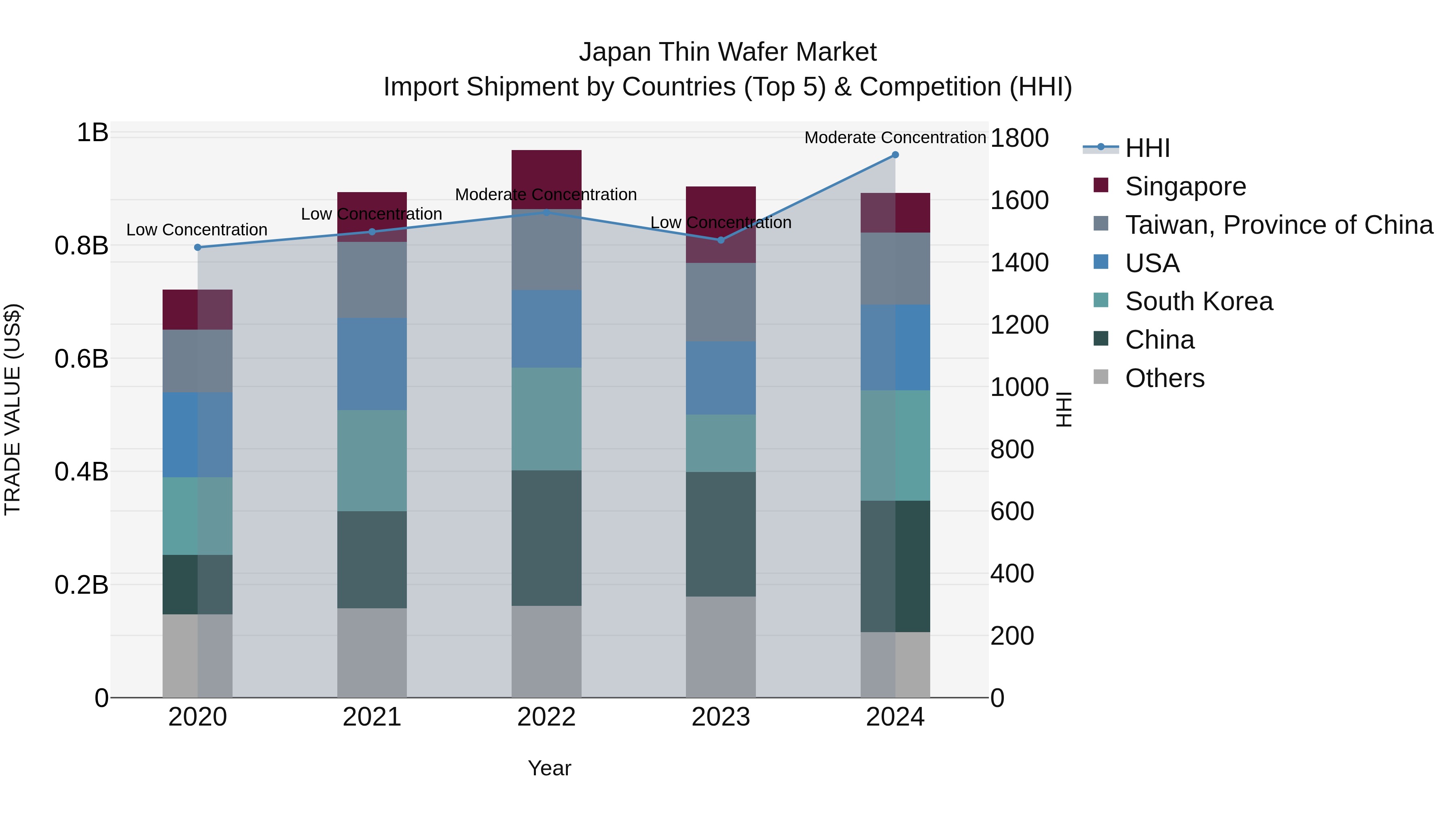
Japan Thin Wafer Market Import Shipment by Countries (Top 5) & Competition (HHI)
The import shipments of thin wafer products in Japan show a diverse sourcing landscape in 2024, with top exporters including China, South Korea, USA, Taiwan, and Singapore. The market experienced a shift from low to moderate concentration in 2024, indicating a slight consolidation among key players. Despite a slight decline in growth rate from 2023 to 2024, the compound annual growth rate (CAGR) for the period 2020-2024 remained steady at 5.45%, reflecting a sustained demand for thin wafer products in the Japanese market.
Japan Thin Wafer Market Overview
The Japan Thin Wafer Market is experiencing steady growth driven by increasing demand for advanced semiconductor applications in consumer electronics, automotive, and industrial sectors. Thin wafer technology enables higher performance and efficiency in electronic devices, leading to its adoption in various end-use industries. Key players in the market are focusing on R&D activities to develop innovative processes and materials for thin wafer production, enhancing product quality and performance. The market is also witnessing collaborations and partnerships among manufacturers to expand their market presence and cater to the growing demand for thin wafers in Japan. With the rising trend of miniaturization and integration of electronic components, the Japan Thin Wafer Market is expected to continue its growth trajectory in the coming years.
Japan Thin Wafer Market Trends and Opportunities
The Japan Thin Wafer Market is experiencing significant growth driven by the increasing demand for advanced semiconductor applications such as 5G, IoT, and artificial intelligence. Key trends in the market include the adoption of advanced packaging technologies, the development of ultra-thin wafers for improved performance, and the shift towards smaller form factors. Opportunities lie in the development of innovative manufacturing processes to produce thinner wafers while maintaining high yields and quality. Additionally, collaborations between semiconductor manufacturers and equipment suppliers to enhance production capabilities and meet the growing demand for thin wafer technology present promising prospects in the Japan Thin Wafer Market.
Japan Thin Wafer Market Challenges
The Japan Thin Wafer Market faces challenges such as high production costs due to the complex manufacturing processes involved in producing thin wafers, as well as the need for specialized equipment and expertise. Additionally, the demand for thinner wafers continues to increase, driving the need for continuous innovation and technological advancements to meet these requirements. Competition from other markets and the pressure to deliver high-quality products consistently also pose challenges for companies operating in this sector. Furthermore, ensuring the reliability and durability of thin wafers while maintaining cost-effectiveness remains a key concern for market players in Japan. Overall, navigating these challenges requires strategic planning, investment in research and development, and a deep understanding of market trends and customer needs.
Japan Thin Wafer Market Drivers
The Japan Thin Wafer Market is being driven by several key factors, including the growing demand for advanced semiconductor devices in various applications such as consumer electronics, automotive, and healthcare. Technological advancements in wafer processing techniques, such as laser processing and thinning processes, are also contributing to market growth by enabling the production of thinner wafers with improved performance characteristics. Additionally, the increasing adoption of wafer-level packaging solutions and the shift towards 3D integration technologies are further driving the demand for thin wafers in Japan. The focus on reducing energy consumption and achieving higher levels of integration in electronic devices is driving the need for thinner and smaller wafers, thereby fueling market expansion in Japan.
Japan Thin Wafer Market Government Policies
In Japan, the government has introduced various policies aimed at promoting the growth of the thin wafer market. These policies include incentives for research and development in thin wafer technology, as well as initiatives to support the adoption of thin wafer manufacturing processes by local companies. Additionally, the government has implemented measures to enhance the competitiveness of the thin wafer industry through investments in infrastructure and training programs for skilled workers. Furthermore, there are regulations in place to ensure the sustainability and environmental friendliness of thin wafer production processes. Overall, the Japanese government`s policies are focused on driving innovation, increasing efficiency, and fostering the growth of the thin wafer market in the country.
Japan Thin Wafer Market Future Outlook
The Japan Thin Wafer Market is poised for significant growth in the coming years, driven by increasing demand for advanced electronic devices such as smartphones, tablets, and wearables. With the growing emphasis on miniaturization and performance enhancement in the semiconductor industry, thin wafers are becoming increasingly important for manufacturers seeking to produce smaller, faster, and more energy-efficient chips. Additionally, the development of new technologies such as 5G, Internet of Things (IoT), and artificial intelligence (AI) is expected to further boost demand for thin wafers in Japan. As a result, market players are likely to invest in research and development activities to innovate and enhance their product offerings to cater to the evolving needs of the industry, positioning Japan as a key player in the global thin wafer market.
Key Highlights of the Report:
- Japan Thin Wafer Market Outlook
- Market Size of Japan Thin Wafer Market, 2024
- Forecast of Japan Thin Wafer Market, 2031
- Historical Data and Forecast of Japan Thin Wafer Revenues & Volume for the Period 2021 - 2031
- Japan Thin Wafer Market Trend Evolution
- Japan Thin Wafer Market Drivers and Challenges
- Japan Thin Wafer Price Trends
- Japan Thin Wafer Porter's Five Forces
- Japan Thin Wafer Industry Life Cycle
- Historical Data and Forecast of Japan Thin Wafer Market Revenues & Volume By Wafer Size for the Period 2021 - 2031
- Historical Data and Forecast of Japan Thin Wafer Market Revenues & Volume By 125 mm for the Period 2021 - 2031
- Historical Data and Forecast of Japan Thin Wafer Market Revenues & Volume By 200 mm for the Period 2021 - 2031
- Historical Data and Forecast of Japan Thin Wafer Market Revenues & Volume By 300 mm for the Period 2021 - 2031
- Historical Data and Forecast of Japan Thin Wafer Market Revenues & Volume By Process for the Period 2021 - 2031
- Historical Data and Forecast of Japan Thin Wafer Market Revenues & Volume By Temporary Bonding & Debonding for the Period 2021 - 2031
- Historical Data and Forecast of Japan Thin Wafer Market Revenues & Volume By Carrier-less/Taiko Process for the Period 2021 - 2031
- Historical Data and Forecast of Japan Thin Wafer Market Revenues & Volume By Application for the Period 2021 - 2031
- Historical Data and Forecast of Japan Thin Wafer Market Revenues & Volume By MEMS for the Period 2021 - 2031
- Historical Data and Forecast of Japan Thin Wafer Market Revenues & Volume By CIS for the Period 2021 - 2031
- Historical Data and Forecast of Japan Thin Wafer Market Revenues & Volume By Memory for the Period 2021 - 2031
- Historical Data and Forecast of Japan Thin Wafer Market Revenues & Volume By RF Devices for the Period 2021 - 2031
- Historical Data and Forecast of Japan Thin Wafer Market Revenues & Volume By LED for the Period 2021 - 2031
- Historical Data and Forecast of Japan Thin Wafer Market Revenues & Volume By Interposer for the Period 2021 - 2031
- Historical Data and Forecast of Japan Thin Wafer Market Revenues & Volume By Logic for the Period 2021 - 2031
- Historical Data and Forecast of Japan Thin Wafer Market Revenues & Volume By Others for the Period 2021 - 2031
- Japan Thin Wafer Import Export Trade Statistics
- Market Opportunity Assessment By Wafer Size
- Market Opportunity Assessment By Process
- Market Opportunity Assessment By Application
- Japan Thin Wafer Top Companies Market Share
- Japan Thin Wafer Competitive Benchmarking By Technical and Operational Parameters
- Japan Thin Wafer Company Profiles
- Japan Thin Wafer Key Strategic Recommendations
Frequently Asked Questions About the Market Study (FAQs):
6Wresearch actively monitors the Japan Thin Wafer Market and publishes its comprehensive annual report, highlighting emerging trends, growth drivers, revenue analysis, and forecast outlook. Our insights help businesses to make data-backed strategic decisions with ongoing market dynamics. Our analysts track relevent industries related to the Japan Thin Wafer Market, allowing our clients with actionable intelligence and reliable forecasts tailored to emerging regional needs.
Yes, we provide customisation as per your requirements. To learn more, feel free to contact us on sales@6wresearch.com
1 Executive Summary |
2 Introduction |
2.1 Key Highlights of the Report |
2.2 Report Description |
2.3 Market Scope & Segmentation |
2.4 Research Methodology |
2.5 Assumptions |
3 Japan Thin Wafer Market Overview |
3.1 Japan Country Macro Economic Indicators |
3.2 Japan Thin Wafer Market Revenues & Volume, 2021 & 2031F |
3.3 Japan Thin Wafer Market - Industry Life Cycle |
3.4 Japan Thin Wafer Market - Porter's Five Forces |
3.5 Japan Thin Wafer Market Revenues & Volume Share, By Wafer Size , 2021 & 2031F |
3.6 Japan Thin Wafer Market Revenues & Volume Share, By Process , 2021 & 2031F |
3.7 Japan Thin Wafer Market Revenues & Volume Share, By Application , 2021 & 2031F |
4 Japan Thin Wafer Market Dynamics |
4.1 Impact Analysis |
4.2 Market Drivers |
4.2.1 Increasing demand for consumer electronics in Japan |
4.2.2 Technological advancements leading to thinner wafers with enhanced performance |
4.2.3 Growing adoption of thin wafers in industries like automotive and healthcare |
4.3 Market Restraints |
4.3.1 High initial investment required for manufacturing thin wafers |
4.3.2 Challenges in achieving uniformity and reliability in thin wafer production |
4.3.3 Environmental concerns related to the manufacturing processes of thin wafers |
5 Japan Thin Wafer Market Trends |
6 Japan Thin Wafer Market, By Types |
6.1 Japan Thin Wafer Market, By Wafer Size |
6.1.1 Overview and Analysis |
6.1.2 Japan Thin Wafer Market Revenues & Volume, By Wafer Size , 2021 - 2031F |
6.1.3 Japan Thin Wafer Market Revenues & Volume, By 125 mm, 2021 - 2031F |
6.1.4 Japan Thin Wafer Market Revenues & Volume, By 200 mm, 2021 - 2031F |
6.1.5 Japan Thin Wafer Market Revenues & Volume, By 300 mm, 2021 - 2031F |
6.2 Japan Thin Wafer Market, By Process |
6.2.1 Overview and Analysis |
6.2.2 Japan Thin Wafer Market Revenues & Volume, By Temporary Bonding & Debonding , 2021 - 2031F |
6.2.3 Japan Thin Wafer Market Revenues & Volume, By Carrier-less/Taiko Process, 2021 - 2031F |
6.3 Japan Thin Wafer Market, By Application |
6.3.1 Overview and Analysis |
6.3.2 Japan Thin Wafer Market Revenues & Volume, By MEMS, 2021 - 2031F |
6.3.3 Japan Thin Wafer Market Revenues & Volume, By CIS, 2021 - 2031F |
6.3.4 Japan Thin Wafer Market Revenues & Volume, By Memory, 2021 - 2031F |
6.3.5 Japan Thin Wafer Market Revenues & Volume, By RF Devices, 2021 - 2031F |
6.3.6 Japan Thin Wafer Market Revenues & Volume, By LED, 2021 - 2031F |
6.3.7 Japan Thin Wafer Market Revenues & Volume, By Interposer, 2021 - 2031F |
6.3.8 Japan Thin Wafer Market Revenues & Volume, By Others, 2021 - 2031F |
6.3.9 Japan Thin Wafer Market Revenues & Volume, By Others, 2021 - 2031F |
7 Japan Thin Wafer Market Import-Export Trade Statistics |
7.1 Japan Thin Wafer Market Export to Major Countries |
7.2 Japan Thin Wafer Market Imports from Major Countries |
8 Japan Thin Wafer Market Key Performance Indicators |
8.1 Average thickness reduction percentage of thin wafers produced |
8.2 Adoption rate of thin wafers in new applications or industries |
8.3 Number of patents filed for innovations in thin wafer technology |
8.4 Energy efficiency improvements in thin wafer manufacturing processes |
9 Japan Thin Wafer Market - Opportunity Assessment |
9.1 Japan Thin Wafer Market Opportunity Assessment, By Wafer Size , 2021 & 2031F |
9.2 Japan Thin Wafer Market Opportunity Assessment, By Process , 2021 & 2031F |
9.3 Japan Thin Wafer Market Opportunity Assessment, By Application , 2021 & 2031F |
10 Japan Thin Wafer Market - Competitive Landscape |
10.1 Japan Thin Wafer Market Revenue Share, By Companies, 2024 |
10.2 Japan Thin Wafer Market Competitive Benchmarking, By Operating and Technical Parameters |
11 Company Profiles |
12 Recommendations |
13 Disclaimer |
Export potential assessment - trade Analytics for 2030
Export potential enables firms to identify high-growth global markets with greater confidence by combining advanced trade intelligence with a structured quantitative methodology. The framework analyzes emerging demand trends and country-level import patterns while integrating macroeconomic and trade datasets such as GDP and population forecasts, bilateral import–export flows, tariff structures, elasticity differentials between developed and developing economies, geographic distance, and import demand projections. Using weighted trade values from 2020–2024 as the base period to project country-to-country export potential for 2030, these inputs are operationalized through calculated drivers such as gravity model parameters, tariff impact factors, and projected GDP per-capita growth. Through an analysis of hidden potentials, demand hotspots, and market conditions that are most favorable to success, this method enables firms to focus on target countries, maximize returns, and global expansion with data, backed by accuracy.
By factoring in the projected importer demand gap that is currently unmet and could be potential opportunity, it identifies the potential for the Exporter (Country) among 190 countries, against the general trade analysis, which identifies the biggest importer or exporter.
To discover high-growth global markets and optimize your business strategy:
Click Here
Pricing
- Single User License$ 1,995
- Department License$ 2,400
- Site License$ 3,120
- Global License$ 3,795

Search
Thought Leadership and Analyst Meet


Our Clients
Latest Reports
- Taiwan Food Delivery Platform Market (2026-2032) | Companies, Outlook, Analysis, Trends, Value, Revenue, Segmentation, Share, Forecast, Competitive Landscape, Growth, Size & Forecast
- United Kingdom (UK) Long-term Care Insurance Market (2026-2032) | Growth, Share, Consumer Insights, Drivers, Opportunities, Competition, Pricing Analysis, Segments, Restraints, Companies, Competitive, Value, Outlook, Size, Demand, Analysis, Challenges, Strategic Insights, Investment Trends, Revenue, Trends, Supply, Forecast
- United Kingdom (UK) Long Term Care Market (2026-2032) | Companies, Outlook, Analysis, Trends, Value, Revenue, Segmentation, Share, Forecast, Competitive Landscape, Growth, Size & Forecast
- Iraq Insulation and Waterproofing Market (2026-2032) | Outlook, Drivers, Growth, Size, Share, Industry, Revenue, Trends, Demand, Competitive, Strategic Insights, Opportunities, Segments, Companies, Challenges, Strategy, Consumer Insights, Analysis, Investment Trends, Value, Segmentation, Forecast, Restraints
- India Switchgear Market Outlook (2026-2032) | Size, Share, Trends, Growth, Revenue, Forecast, Analysis, Value, Outlook
- Pakistan Contraceptive Implants Market (2025-2031) | Demand, Growth, Size, Share, Industry, Pricing Analysis, Competitive, Strategic Insights, Strategy, Consumer Insights, Analysis, Investment Trends, Opportunities, Revenue, Segments, Value, Segmentation, Supply, Forecast, Restraints, Outlook, Competition, Drivers, Trends, Companies, Challenges
- Sri Lanka Packaging Market (2026-2032) | Outlook, Competition, Drivers, Trends, Demand, Pricing Analysis, Competitive, Strategic Insights, Companies, Challenges, Strategy, Consumer Insights, Analysis, Investment Trends, Opportunities, Growth, Size, Share, Industry, Revenue, Segments, Value, Segmentation, Supply, Forecast, Restraints
- India Kids Watches Market (2026-2032) | Strategy, Consumer Insights, Analysis, Investment Trends, Opportunities, Growth, Size, Share, Industry, Revenue, Segments, Value, Segmentation, Supply, Forecast, Restraints, Outlook, Competition, Drivers, Trends, Demand, Pricing Analysis, Competitive, Strategic Insights, Companies, Challenges
- Saudi Arabia Core Assurance Service Market (2025-2031) | Strategy, Consumer Insights, Analysis, Investment Trends, Opportunities, Growth, Size, Share, Industry, Revenue, Segments, Value, Segmentation, Supply, Forecast, Restraints, Outlook, Competition, Drivers, Trends, Demand, Pricing Analysis, Competitive, Strategic Insights, Companies, Challenges
- Romania Uninterruptible Power Supply (UPS) Market (2026-2032) | Industry, Analysis, Revenue, Size, Forecast, Outlook, Value, Trends, Share, Growth & Companies
Industry Events and Analyst Meet

India EV Show 2026

EV tech India Expo 2026

Auto Tech Asia 2026

Battery Tech India 2026

Smart Production Solutions Guangzhou 2026
Whitepaper
- Middle East & Africa Commercial Security Market Click here to view more.
- Middle East & Africa Fire Safety Systems & Equipment Market Click here to view more.
- GCC Drone Market Click here to view more.
- Middle East Lighting Fixture Market Click here to view more.
- GCC Physical & Perimeter Security Market Click here to view more.
6WResearch In News
- Doha a strategic location for EV manufacturing hub: IPA Qatar
- Demand for luxury TVs surging in the GCC, says Samsung
- Empowering Growth: The Thriving Journey of Bangladesh’s Cable Industry
- Demand for luxury TVs surging in the GCC, says Samsung
- Video call with a traditional healer? Once unthinkable, it’s now common in South Africa
- Intelligent Buildings To Smooth GCC’s Path To Net Zero