South Korea 2.5D and 3D Semiconductor Packaging Market (2026-2032) | Strategy, Analysis, Companies, Growth, Competition, Restraints, Opportunities, Trends, Supply, Challenges, Segmentation, Outlook, Value, Industry, Share, Revenue, Consumer Insights, Size, Strategic Insights, Forecast, Pricing Analysis, Segments, Drivers, Investment Trends, Demand, Competitive
Market Forecast By Packaging Technology (2.5 D, 3D), By Application (Memory, Logic, MEMS), By Material Type (Silicon, Glass, Organic Substrate), By End User (Automotive, Consumer Electronics) And Competitive Landscape
| Product Code: ETC11433514 | Publication Date: Apr 2025 | Updated Date: May 2026 | Product Type: Market Research Report | |
| Publisher: 6Wresearch | Author: Bhawna Singh | No. of Pages: 65 | No. of Figures: 34 | No. of Tables: 19 |
South Korea 2.5D and 3D Semiconductor Packaging Market Growth Rate ETC11433514
According to 6Wresearch internal database and industry insights, the South Korea 2.5D and 3D Semiconductor Packaging Market is projected to grow at a compound annual growth rate (CAGR) of 14.8% during the forecast period (2026-2032).
South Korea 2.5D and 3D Semiconductor Packaging Market Year-wise Growth Rate and Key Drivers
This graph highlights how the South Korea 2.5D and 3D Semiconductor Packaging Market has steadily grown over the past five years, supported by major growth factors.
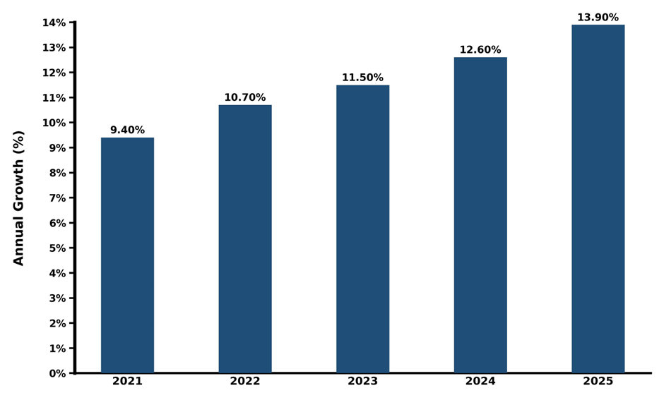
The table below presents the year‑wise growth rates along with the key drivers influencing the market
| Year | Est. Annual Growth (%) | Growth Drivers |
| 2021 | 9.4% | Surging demand for High Bandwidth Memory (HBM) in data centers |
| 2022 | 10.7% | Rapid expansion of domestic foundry capabilities for AI chips |
| 2023 | 11.5% | Increased adoption of Chip-on-Wafer-on-Substrate (CoWoS) technologies |
| 2024 | 12.6% | Integration of advanced packaging in next-gen consumer electronics |
| 2025 | 13.9% | Government subsidies for domestic advanced packaging R&D centers |
Topics Covered in the South Korea 2.5D and 3D Semiconductor Packaging Market Report
The South Korea 2.5D and 3D Semiconductor Packaging Market report thoroughly covers the market by Packaging Technology, Application, Material Type and End User. The market report provides an unbiased and detailed analysis of ongoing market trends, opportunities/high growth areas, and market drivers, which help stakeholders devise and align their market strategies according to the current and future market dynamics.
South Korea 2.5D and 3D Semiconductor Packaging Market Highlights
| Report Name |
South Korea 2.5D and 3D Semiconductor Packaging Market |
| Forecast period | 2026-2032 |
| CAGR | 14.8% |
| Market Size |
Logic & HBM Computing Segments |
South Korea 2.5D and 3D Semiconductor Packaging Market Synopsis
South Korea 2.5D and 3D Semiconductor Packaging Market is anticipated to record notable growth due to the escalating demand for high-performance computing, the proliferation of artificial intelligence, and the strategic shift toward heterogeneous integration in chip manufacturing. In general, there has been a lot of development taking place within the local semiconductor ecosystem due to the high investments being made by top companies in developing TSVs and Wafer-Level Packaging. This is done in order to bypass any barriers set forth by Moore’s Law. In addition, due to the abundance of world-class memory producers in the region, the shift towards adopting 3D stacked memory has been quite smooth.
Evaluation of Growth Drivers in the South Korea 2.5D and 3D Semiconductor Packaging Market (2026-2032)
Below mentioned are some prominent drivers and their influence on the market dynamics:
| Drivers | Primary Segments Affected | Why it Matters (Evidence) |
| Proliferation of Generative AI | 3D Packaging, Logic | AI workloads require massive bandwidth provided by 3D stacked memory and logic integration. |
| Expansion of 5G/6G Networks | 2.5D Packaging, MEMS | High-frequency communication modules necessitate compact, low-latency packaging solutions. |
| Automotive Electrification | 2.5D Packaging, Automotive | Sophisticated ADAS systems drive the need for reliable, high-density power and logic packaging. |
| Rise of Chiplet Architectures | All Types, Consumer Electronics | Manufacturers are moving from monolithic dies to chiplets, increasing demand for 2.5D interposers. |
| Supportive Industrial Policies | All Types, Memory | Strategic national roadmaps provide tax credits and infrastructure for advanced packaging fabs. |
South Korea 2.5D and 3D Semiconductor Packaging Market is expected to grow at the CAGR of 14.8% during the forecast period of 2026-2032. Growth is driven by improving oncology care, increasing awareness of male breast cancer, and expanding medicine availability. Additional contributions come from international healthcare support groups and government programs aimed at strengthening diagnostic and treatment capabilities across the country.
Evaluation of Restraints in the South Korea 2.5D and 3D Semiconductor Packaging Market
Below mentioned are some major restraints and their influence on the market dynamics:
| Restraints | Primary Segments Affected | What This Means (Evidence) |
| High Technical Complexity | 3D Packaging, Silicon | The intricate nature of TSV and micro-bumping leads to lower yields and higher initial R&D costs. |
| Thermal Challenges | 3D Integration, Logic | The density created through vertical integration results in substantial thermal issues. |
| Expensive Start-up Costs | All Advanced Packaging Processes, Foundry | The creation of advanced packaging lines is extremely costly. |
| Supply Chain Constraints | Materials, Organic Substrate | The dependency on particular substrates imported from abroad may pose production constraints. |
| Export Restrictions Due to Geopolitics | All Advanced Packaging Processes, Automotive | The export limitations on advanced machinery may affect the import of lithography equipment |
South Korea 2.5D and 3D Semiconductor Packaging Market Challenges
Irrespective of massive growth and development, the Market faces several challenges such as high production costs associated with silicon interposers, thermal dissipation hurdles in vertically stacked dies, and the necessity for extreme precision in wafer bonding. In addition to this, the South Korea 2.5D and 3D Semiconductor Packaging Market Growth is occasionally hindered by the scarcity of specialized workforce talent capable of managing hybrid bonding processes and the intensive capital requirements needed to maintain competitive technological parity with global peers.
South Korea 2.5D and 3D Semiconductor Packaging Market Trends
Key trends evaluating the landscape of the South Korea 2.5D and 3D Semiconductor Packaging Market are:
- Hybrid Bonding Adoption: The industry is transitioning from traditional micro-bumps to copper-to-copper hybrid bonding to achieve higher interconnect density and better electrical performance.
- Glass Substrate Expansion: The industry is investigating the possibility of replacing silicon with glass substrates for better signal integrity and a reduction in the thickness of the high-performance modules.
- AI-PC and AI-Smartphone Processor Development: The industry has seen a shift towards creating NPU-dominant processors with fast memory using 2.5D packaging to perform AI functions on the device.
- Eco-Friendly Approach in Manufacturing: There has been a move towards sustainable manufacturing processes through the use of green CMP slurries and energy-efficient cleanroom technology.
Investment Opportunities in the South Korea 2.5D and 3D Semiconductor Packaging Market
Some notable investment areas in the South Korean 2.5D and 3D Semiconductor Packaging Market are:
- Automated Optical Inspection: Development of AOI systems that can achieve high yields in 3D stack architectures.
- Local Materials Supply Chain: Creation of local manufacturing capabilities for high purity photoresist and specialty gases needed only for TSV processing.
- Heterogeneous Integration: Research & development of startups that focus on developing interposer technologies and multi-die orchestration software to lower power consumption in data centers.
- Automotive Grade Packaging: Setting up dedicated lines for robust 2.5D semiconductor packaging that can withstand the harsh environmental conditions inside autonomous vehicles.
Top 5 Leading Players in the South Korea 2.5D and 3D Semiconductor Packaging Market
Some leading players operating in the South Korea 2.5D and 3D Semiconductor Packaging Market include:
1. Samsung Electronics Co., Ltd.
| Company Name | Samsung Electronics Co., Ltd. |
|---|---|
| Established Year | 1969 |
| Headquarters | Suwon, South Korea |
| Official Website | Click Here |
Samsung is a dominant force providing end-to-end advanced packaging services including I-Cube and X-Cube technologies for high-performance computing applications and advanced memory integration.
2. SK Hynix Inc.
| Company Name | SK Hynix Inc. |
|---|---|
| Established Year | 1983 |
| Headquarters | Icheon, South Korea |
| Official Website | Click Here |
SK Hynix leads the global HBM market, utilizing advanced 3D stacking and Mass Reflow Molded Underfill (MR-MUF) technology to deliver industry-leading memory solutions.
3. Amkor Technology Korea
| Company Name | Amkor Technology Korea |
|---|---|
| Established Year | 1968 |
| Headquarters | Seoul, South Korea (Regional) |
| Official Website | Click Here |
Amkor provides extensive OSAT services in South Korea, specializing in wafer-level packaging and 2.5D/3D integration for mobile and automotive semiconductor clients.
4. Hana Micron Inc.
| Company Name | Hana Micron Inc. |
|---|---|
| Established Year | 2001 |
| Headquarters | Asan, South Korea |
| Official Website | - |
Hana Micron offers specialized back-end semiconductor services, focusing on memory packaging and expanding its footprint in advanced 2.5D solutions for diverse industries.
5. LB Semicon Co., Ltd.
| Company Name | LB Semicon Co., Ltd. |
|---|---|
| Established Year | 2000 |
| Headquarters | Pyeongtaek, South Korea |
| Official Website | Click Here |
LB Semicon provides gold bumping and wafer-level chip scale packaging (WLCSP) services, playing a critical role in the display and sensor packaging ecosystem.
Government Regulations Introduced in the South Korea 2.5D and 3D Semiconductor Packaging Market
According to South Korean Government Data, the “K-Semiconductor Strategy” that was introduced in 2021 and extended to 2024 provides huge tax incentives for R&D activities and capital expenditures for advanced packaging industries. The Ministry of Trade, Industry, and Energy (MOTIE) has designated 2.5D and 3D technology development as “National Strategic Technologies,” making it possible for companies to receive simplified regulatory processes and specialised energy facilities. Moreover, the introduction of the Special Act on Strengthening and Protecting National Strategic Industry Competitiveness has helped the government create an IP protection system and conduct collaborative research among local universities and semiconductor giants.
Future Insights of the South Korea 2.5D and 3D Semiconductor Packaging Market
The outlook for the South Korea 2.5D and 3D Semiconductor Packaging Industry is promising due to the impact of the rapid transition toward 6G technology and the exponential growth of edge computing. The Growth will be further bolstered by the increasing integration of silicon photonics and co-packaged optics, which are essential for meeting the data throughput demands of the future, while continuous investments in domestic OSAT facilities ensure a resilient and technologically superior semiconductor supply chain.
Market Segmentation Analysis
The report offers a comprehensive study of the subsequent market segments and their leading categories:
3D Packaging Technology to Dominate the Market- By Packaging Technology
According to Nikita, Senior Research Analyst, 6Wresearch, the 3D Packaging category is expected to play a leading role in the South Korea 2.5D and 3D Semiconductor Packaging Market Share. The relentless push for miniaturisation and the necessity to reduce the physical footprint of chips while maximising performance have driven the rapid adoption of 3D stacking. Moreover, the critical demand for High Bandwidth Memory in AI servers ensures that vertical integration remains the primary focus for technology leaders in the region.
Key Attractiveness of the Report
- 10 Years of Market Numbers.
- Historical Data Starting from 2022 to 2025.
- Base Year: 2025.
- Forecast Data until 2032.
- Key Performance Indicators Impacting the Market.
- Major Upcoming Developments and Projects.
Key Highlights of the Report:
- South Korea 2.5D and 3D Semiconductor Packaging Market Outlook
- Market Size of South Korea 2.5D and 3D Semiconductor Packaging Market, 2025
- Forecast of South Korea 2.5D and 3D Semiconductor Packaging Market, 2032
- Historical Data and Forecast of South Korea 2.5D and 3D Semiconductor Packaging Revenues & Volume for the Period 2022-2032
- South Korea 2.5D and 3D Semiconductor Packaging Market Trend Evolution
- South Korea 2.5D and 3D Semiconductor Packaging Market Drivers and Challenges
- South Korea 2.5D and 3D Semiconductor Packaging Price Trends
- South Korea 2.5D and 3D Semiconductor Packaging Porter's Five Forces
- South Korea 2.5D and 3D Semiconductor Packaging Industry Life Cycle
- Historical Data and Forecast of South Korea 2.5D and 3D Semiconductor Packaging Market Revenues & Volume By Packaging Technology for the Period 2022-2032
- Historical Data and Forecast of South Korea 2.5D and 3D Semiconductor Packaging Market Revenues & Volume By 2.5 D for the Period 2022-2032
- Historical Data and Forecast of South Korea 2.5D and 3D Semiconductor Packaging Market Revenues & Volume By 3D for the Period 2022-2032
- Historical Data and Forecast of South Korea 2.5D and 3D Semiconductor Packaging Market Revenues & Volume By Application for the Period 2022-2032
- Historical Data and Forecast of South Korea 2.5D and 3D Semiconductor Packaging Market Revenues & Volume By Memory for the Period 2022-2032
- Historical Data and Forecast of South Korea 2.5D and 3D Semiconductor Packaging Market Revenues & Volume By Logic for the Period 2022-2032
- Historical Data and Forecast of South Korea 2.5D and 3D Semiconductor Packaging Market Revenues & Volume By MEMS for the Period 2022-2032
- Historical Data and Forecast of South Korea 2.5D and 3D Semiconductor Packaging Market Revenues & Volume By Material Type for the Period 2022-2032
- Historical Data and Forecast of South Korea 2.5D and 3D Semiconductor Packaging Market Revenues & Volume By Silicon for the Period 2022-2032
- Historical Data and Forecast of South Korea 2.5D and 3D Semiconductor Packaging Market Revenues & Volume By Glass for the Period 2022-2032
- Historical Data and Forecast of South Korea 2.5D and 3D Semiconductor Packaging Market Revenues & Volume By Organic Substrate for the Period 2022-2032
- Historical Data and Forecast of South Korea 2.5D and 3D Semiconductor Packaging Market Revenues & Volume By End User for the Period 2022-2032
- Historical Data and Forecast of South Korea 2.5D and 3D Semiconductor Packaging Market Revenues & Volume By Automotive for the Period 2022-2032
- Historical Data and Forecast of South Korea 2.5D and 3D Semiconductor Packaging Market Revenues & Volume By Consumer Electronics for the Period 2022-2032
- South Korea 2.5D and 3D Semiconductor Packaging Import Export Trade Statistics
- Market Opportunity Assessment By Packaging Technology
- Market Opportunity Assessment By Application
- Market Opportunity Assessment By Material Type
- Market Opportunity Assessment By End User
- South Korea 2.5D and 3D Semiconductor Packaging Top Companies Market Share
- South Korea 2.5D and 3D Semiconductor Packaging Competitive Benchmarking By Technical and Operational Parameters
- South Korea 2.5D and 3D Semiconductor Packaging Company Profiles
- South Korea 2.5D and 3D Semiconductor Packaging Key Strategic Recommendations
Market Covered
The report offers a comprehensive study of the subsequent market segments:
By Packaging Technology
- 3D Packaging
- 2.5D Packaging
By Application
- Memory
- Logic
- MEMS
By Material Type
- Silicon
- Organic Substrate
- Glass
By End User
- Consumer Electronics
- Automotive
South Korea 2.5D and 3D Semiconductor Packaging Market (2026-2032): FAQs
South Korea 2.5D and 3D Semiconductor Packaging Market is projected to grow at a CAGR of 14.8% between 2026-2032.
The most significant investment potential lies in the development of domestic advanced testing facilities and the localized production of high-precision materials like silicon interposers and specialized bonding chemicals.
The market is led by industry giants including Samsung Electronics, SK Hynix, Amkor Technology, Hana Micron, and LB Semicon.
The most significant trend is the shift toward hybrid bonding and the use of glass substrates to enhance the performance of AI-centric processors.
6Wresearch actively monitors the South Korea 2.5D and 3D Semiconductor Packaging Market and publishes its comprehensive annual report, highlighting emerging trends, growth drivers, revenue analysis, and forecast outlook. Our insights help businesses to make data-backed strategic decisions with ongoing market dynamics. Our analysts track relevent industries related to the South Korea 2.5D and 3D Semiconductor Packaging Market, allowing our clients with actionable intelligence and reliable forecasts tailored to emerging regional needs.
Yes, we provide customisation as per your requirements. To learn more, feel free to contact us on sales@6wresearch.com
| 1 Executive Summary |
| 2 Introduction |
| 2.1 Key Highlights of the Report |
| 2.2 Report Description |
| 2.3 Market Scope & Segmentation |
| 2.4 Research Methodology |
| 2.5 Assumptions |
| 3 South Korea 2.5D and 3D Semiconductor Packaging Market Overview |
| 3.1 South Korea Country Macro Economic Indicators |
| 3.2 South Korea 2.5D and 3D Semiconductor Packaging Market Revenues & Volume, 2022 & 2032F |
| 3.3 South Korea 2.5D and 3D Semiconductor Packaging Market - Industry Life Cycle |
| 3.4 South Korea 2.5D and 3D Semiconductor Packaging Market - Porter's Five Forces |
| 3.5 South Korea 2.5D and 3D Semiconductor Packaging Market Revenues & Volume Share, By Packaging Technology, 2022 & 2032F |
| 3.6 South Korea 2.5D and 3D Semiconductor Packaging Market Revenues & Volume Share, By Application, 2022 & 2032F |
| 3.7 South Korea 2.5D and 3D Semiconductor Packaging Market Revenues & Volume Share, By Material Type, 2022 & 2032F |
| 3.8 South Korea 2.5D and 3D Semiconductor Packaging Market Revenues & Volume Share, By End User, 2022 & 2032F |
| 4 South Korea 2.5D and 3D Semiconductor Packaging Market Dynamics |
| 4.1 Impact Analysis |
| 4.2 Market Drivers |
| 4.2.1 Increasing demand for advanced packaging solutions in the semiconductor industry |
| 4.2.2 Technological advancements in 2.5D and 3D semiconductor packaging |
| 4.2.3 Growing adoption of miniaturized electronic devices driving the need for more efficient packaging solutions |
| 4.3 Market Restraints |
| 4.3.1 High initial investment required for setting up 2.5D and 3D semiconductor packaging facilities |
| 4.3.2 Complexity in design and manufacturing processes leading to longer development cycles |
| 4.3.3 Limited availability of skilled workforce specialized in 2.5D and 3D packaging technologies |
| 5 South Korea 2.5D and 3D Semiconductor Packaging Market Trends |
| 6 South Korea 2.5D and 3D Semiconductor Packaging Market, By Types |
| 6.1 South Korea 2.5D and 3D Semiconductor Packaging Market, By Packaging Technology |
| 6.1.1 Overview and Analysis |
| 6.1.2 South Korea 2.5D and 3D Semiconductor Packaging Market Revenues & Volume, By Packaging Technology, 2022 - 2032F |
| 6.1.3 South Korea 2.5D and 3D Semiconductor Packaging Market Revenues & Volume, By 2.5 D, 2022 - 2032F |
| 6.1.4 South Korea 2.5D and 3D Semiconductor Packaging Market Revenues & Volume, By 3D, 2022 - 2032F |
| 6.2 South Korea 2.5D and 3D Semiconductor Packaging Market, By Application |
| 6.2.1 Overview and Analysis |
| 6.2.2 South Korea 2.5D and 3D Semiconductor Packaging Market Revenues & Volume, By Memory, 2022 - 2032F |
| 6.2.3 South Korea 2.5D and 3D Semiconductor Packaging Market Revenues & Volume, By Logic, 2022 - 2032F |
| 6.2.4 South Korea 2.5D and 3D Semiconductor Packaging Market Revenues & Volume, By MEMS, 2022 - 2032F |
| 6.3 South Korea 2.5D and 3D Semiconductor Packaging Market, By Material Type |
| 6.3.1 Overview and Analysis |
| 6.3.2 South Korea 2.5D and 3D Semiconductor Packaging Market Revenues & Volume, By Silicon, 2022 - 2032F |
| 6.3.3 South Korea 2.5D and 3D Semiconductor Packaging Market Revenues & Volume, By Glass, 2022 - 2032F |
| 6.3.4 South Korea 2.5D and 3D Semiconductor Packaging Market Revenues & Volume, By Organic Substrate, 2022 - 2032F |
| 6.4 South Korea 2.5D and 3D Semiconductor Packaging Market, By End User |
| 6.4.1 Overview and Analysis |
| 6.4.2 South Korea 2.5D and 3D Semiconductor Packaging Market Revenues & Volume, By Automotive, 2022 - 2032F |
| 6.4.3 South Korea 2.5D and 3D Semiconductor Packaging Market Revenues & Volume, By Consumer Electronics, 2022 - 2032F |
| 7 South Korea 2.5D and 3D Semiconductor Packaging Market Import-Export Trade Statistics |
| 7.1 South Korea 2.5D and 3D Semiconductor Packaging Market Export to Major Countries |
| 7.2 South Korea 2.5D and 3D Semiconductor Packaging Market Imports from Major Countries |
| 8 South Korea 2.5D and 3D Semiconductor Packaging Market Key Performance Indicators |
| 8.1 Average number of new patents filed for 2.5D and 3D semiconductor packaging technologies |
| 8.2 Adoption rate of 2.5D and 3D packaging solutions by leading semiconductor manufacturers |
| 8.3 Percentage increase in research and development spending by companies in the semiconductor packaging sector |
| 9 South Korea 2.5D and 3D Semiconductor Packaging Market - Opportunity Assessment |
| 9.1 South Korea 2.5D and 3D Semiconductor Packaging Market Opportunity Assessment, By Packaging Technology, 2022 & 2032F |
| 9.2 South Korea 2.5D and 3D Semiconductor Packaging Market Opportunity Assessment, By Application, 2022 & 2032F |
| 9.3 South Korea 2.5D and 3D Semiconductor Packaging Market Opportunity Assessment, By Material Type, 2022 & 2032F |
| 9.4 South Korea 2.5D and 3D Semiconductor Packaging Market Opportunity Assessment, By End User, 2022 & 2032F |
| 10 South Korea 2.5D and 3D Semiconductor Packaging Market - Competitive Landscape |
| 10.1 South Korea 2.5D and 3D Semiconductor Packaging Market Revenue Share, By Companies, 2025 |
| 10.2 South Korea 2.5D and 3D Semiconductor Packaging Market Competitive Benchmarking, By Operating and Technical Parameters |
| 11 Company Profiles |
| 12 Recommendations |
| 13 Disclaimer |
Global Go To Market Strategy - 2030
Export potential enables firms to identify high-growth global markets with greater confidence by combining advanced trade intelligence with a structured quantitative methodology. The framework analyzes emerging demand trends and country-level import patterns while integrating macroeconomic and trade datasets such as GDP and population forecasts, bilateral import–export flows, tariff structures, elasticity differentials between developed and developing economies, geographic distance, and import demand projections. Using weighted trade values from 2020–2024 as the base period to project country-to-country export potential for 2030, these inputs are operationalized through calculated drivers such as gravity model parameters, tariff impact factors, and projected GDP per-capita growth. Through an analysis of hidden potentials, demand hotspots, and market conditions that are most favorable to success, this method enables firms to focus on target countries, maximize returns, and global expansion with data, backed by accuracy.
By factoring in the projected importer demand gap that is currently unmet and could be potential opportunity, it identifies the potential for the Exporter (Country) among 190 countries, against the general trade analysis, which identifies the biggest importer or exporter.
To discover high-growth global markets and optimize your business strategy:
Click Here
Pricing
- Single User License$ 1,995
- Department License$ 2,400
- Site License$ 3,120
- Global License$ 3,795

Leadership Perspectives from Industry Events
Search
Thought Leadership and Analyst Meet


Our Clients
6WResearch In News
- Doha a strategic location for EV manufacturing hub: IPA Qatar
- Demand for luxury TVs surging in the GCC, says Samsung
- Empowering Growth: The Thriving Journey of Bangladesh’s Cable Industry
- Demand for luxury TVs surging in the GCC, says Samsung
- Video call with a traditional healer? Once unthinkable, it’s now common in South Africa
- Intelligent Buildings To Smooth GCC’s Path To Net Zero
Latest Reports
- Taiwan Airport Wireless Infrastructure Market (2026-2032)
- Vietnam Airport Wireless Infrastructure Market (2026-2032)
- Thailand Airport Wireless Infrastructure Market (2026-2032)
- South Korea Airport Wireless Infrastructure Market (2026-2032)
- Romania Airport Wireless Infrastructure Market (2026-2032)
- Qatar Airport Wireless Infrastructure Market (2026-2032)
- Philippines Airport Wireless Infrastructure Market (2026-2032)
- Japan Airport Wireless Infrastructure Market (2026-2032)
- Taiwan Airport Winter Services Market (2026-2032)
- Vietnam Airport Winter Services Market (2026-2032)
Industry Events and Analyst Meet
HIMTEX 2026

India Refining Summit 2026

India EV Show 2026

EV tech India Expo 2026

Auto Tech Asia 2026
Whitepaper
- Middle East & Africa Commercial Security Market Click here to view more.
- Middle East & Africa Fire Safety Systems & Equipment Market Click here to view more.
- GCC Drone Market Click here to view more.
- Middle East Lighting Fixture Market Click here to view more.
- GCC Physical & Perimeter Security Market Click here to view more.