Japan Scanning Probe Microscopy Market Size & Growth Rate
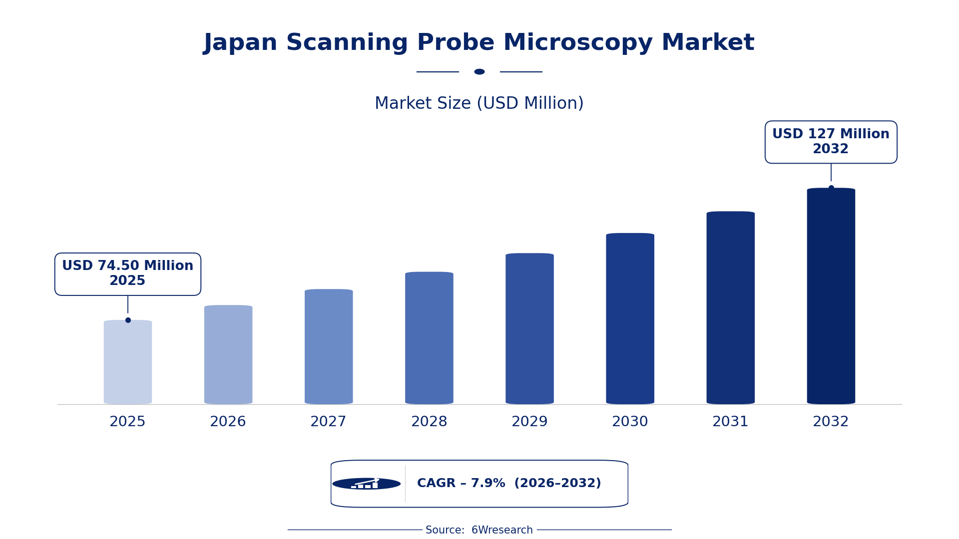
According to 6Wresearch internal database and industry insights, the Japan Scanning Probe Microscopy Market was valued at USD 74.50 Million in 2025 and is projected to reach USD 127 Million by 2032, growing at a CAGR of approximately 7.9% during 2026–2032.
Japan Scanning Probe Microscopy Market Highlights
| Report Metric | Details |
| Report Name | Japan Scanning Probe Microscopy Market (2026-2032) |
| Market Size 2025 | USD 74.50 Million |
| Market Size 2032 | USD 127 Million |
| Absolute Growth 2025–2032 | USD 52.50 Million |
| CAGR 2026–2032 | 7.9% |
| Peak Annual Growth | 8.5% in 2028 |
| Forecast Period | 2026–2032 |
| Historical Data | 2022–2025 |
| Base Year | 2025 |
| Leading Technique Type, 2025 | AFM (Atomic Force) (35% share) |
| Leading Resolution Level, 2025 | Sub-nanometer (37% share) |
| Leading Instrument Format, 2025 | Desktop Benchtop (49% share) |
| Leading End User, 2025 | Semiconductor R&D (35% share) |
| Fastest-Growing Technique Type | Magnetic Force Microscopy (10.8% CAGR) |
| Fastest-Growing Resolution Level | Near-field (10.4% CAGR) |
| Fastest-Growing Instrument Format | Modular Instruments (11.3% CAGR) |
| Fastest-Growing End User | Nanotech Companies (10.5% CAGR) |
| Growing Sector | Nanotechnology |
| Key End Users | University Research Labs, Semiconductor R&D, Nanotech Companies |
Japan Scanning Probe Microscopy Market Year-wise Growth Rate and Key Drivers (2022–2032)
This graph illustrates the annual growth rates of the market from 2022 to 2032, highlighting a steady upward trajectory and projected market expansion over the forecast period.
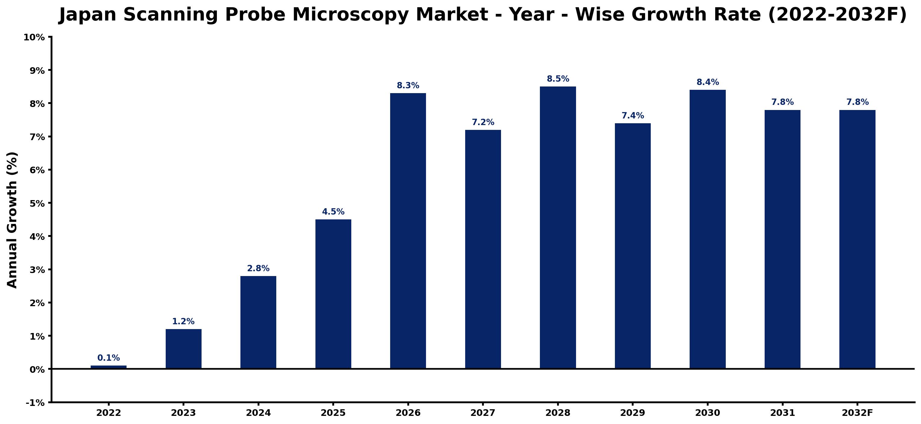
The yearly estimates that follow link every growth rate to its principal driver, so readers can see why the pace changed in each period.
| Year | Estimated Annual Growth (%) | Market Rationale |
| 2022 | 0.1 | The market exhibited minimal growth due to limited investment in advanced research technologies. |
| 2023 | 1.2 | Demand increased as more university research labs began utilising SPM technology. |
| 2024 | 2.8 | Growth accelerated as semiconductor R&D activities expanded in the Tokyo region. |
| 2025 | 4.5 | The market reached a historical peak driven by advancements in nanotechnology applications. |
| 2026 | 8.3 | Demand surged as the semiconductor industry sought improved imaging techniques. |
| 2027 | 7.2 | Growth slowed slightly as capacity constraints began to affect supply. |
| 2028 | 8.5 | The market peaked with heightened investments in advanced materials research. |
| 2029 | 7.4 | A slowdown occurred as growth stabilised after reaching peak levels. |
| 2030 | 8.4 | Demand rebounded with renewed focus on nanotech applications in various sectors. |
| 2031 | 7.8 | Growth decelerated as market saturation started to take effect. |
| 2032 | 7.8 | The market is expected to maintain steady growth driven by ongoing research initiatives. |
Note: Market size estimations and growth projections presented in this report are based on 6Wresearch's proprietary forecasting methodology, utilizing the latest available industry data, government publications, and primary research inputs.
Japan Scanning Probe Microscopy Market Synopsis
Scanning Probe Microscopy (SPM) is a nanoscale imaging technology essential for materials characterization, semiconductor research, and nanotechnology applications. Demand arises from university research labs and semiconductor R&D facilities. The Japan Scanning Probe Microscopy Market is expanding due to increased investment in advanced materials and the promotion of nanotechnology through the 'Moonshot R&D Program'. With over 100 university labs employing SPM, the market is set for continued growth as research activities intensify and funding increases.
Market Dynamics Impact Analysis (2026–2032)
| Factor | Type | Impact | Primary Segment Affected |
| Growing investment in semiconductor R&D | Driver | High | Semiconductor R&D |
| Rising demand for advanced materials characterization | Driver | High | Materials Science Institutes |
| Emerging opportunities in nanotechnology applications | Opportunity | High | Nanotech Companies |
| Increased funding for university research initiatives | Opportunity | Medium | University Research Labs |
| High costs associated with SPM equipment | Restraint | High | AFM (Atomic Force) |
| Limited availability of skilled technicians | Restraint | Medium | AFM (Atomic Force) |
| Compliance with stringent manufacturing standards | Challenge | High | AFM (Atomic Force) |
| Capacity constraints in production facilities | Challenge | Medium | AFM (Atomic Force) |
Evaluation of Drivers in Japan Scanning Probe Microscopy Market (2026–2032)
The main growth drivers and the segments they affect most are set out below.
| Drivers | Primary Segment Affected | Why It Matters (Evidence) |
| Increased funding for semiconductor research initiatives | Semiconductor R&D | The Tokyo region has seen a surge in funding, leading to more SPM purchases for advanced imaging. |
| Growing demand for nanoscale imaging in materials research | Materials Science Institutes | With over 100 university labs using SPM, the need for advanced imaging techniques has risen. |
| Rising interest in nanotechnology applications | Nanotech Companies | SPM technology is used in over 50% of nanotech companies, driving demand for advanced solutions. |
| Expansion of university research programs | University Research Labs | The University of Tokyo's dedicated SPM facility supports increased demand for advanced microscopy. |
| Adoption of ISO 9001 standards in manufacturing | AFM (Atomic Force) | Compliance with these standards improves product quality, encouraging more purchases. |
Several shifts outside the market lift sales. The demand for nanoscale imaging in materials research is growing, with over 100 university labs utilising SPM technology. Interest in nanotechnology applications drives demand, as SPM is widely used in the sector. The University of Tokyo's dedicated SPM facility supports the need for advanced microscopy, while compliance with ISO 9001 standards improves product quality, further encouraging purchases.
Evaluation of Restraints in Japan Scanning Probe Microscopy Market
Below are the constraints most often cited by buyers and suppliers, with the segment each affects.
| Market Restraint | Primary Segment Affected | Why It Matters (Evidence) |
| High costs associated with acquiring SPM equipment | AFM (Atomic Force) | The initial investment for SPM systems can exceed USD 100,000, limiting access for smaller labs. |
| Limited availability of skilled technicians for SPM operation | AFM (Atomic Force) | The shortage of trained professionals can delay project timelines and increase operational costs. |
| Compliance with stringent manufacturing standards | AFM (Atomic Force) | Adhering to regulations such as the PRTR Law increases operational complexity and costs. |
| Dependence on specific materials for SPM production | AFM (Atomic Force) | Supply chain disruptions can affect the availability of critical components for SPM systems. |
| Market saturation in established sectors | AFM (Atomic Force) | As the market matures, growth opportunities may diminish, leading to increased competition. |
Japan Scanning Probe Microscopy Market Challenges
Producers of scanning probe microscopy technology face challenges arising from rapid advancements in imaging techniques, necessitating constant innovation. This issue is prevalent in Japan due to over 100 university research labs demanding cutting-edge solutions, causing delays in product development that can last up to six months. Supply chain disruptions also affect manufacturers, as reliance on specific components from limited suppliers can halt production, resulting in significant revenue loss. Increased competition from global players compels local manufacturers to reduce prices, ultimately raising costs for buyers seeking high-quality SPM solutions.
Trends in the Japan Scanning Probe Microscopy Market
The shifts below are changing how Japan Scanning Probe Microscopy Market products are bought and supplied.
- Shift from Traditional to Advanced Imaging Techniques: In 2023, Japan hosted the International Conference on Scanning Probe Microscopy, showcasing a shift towards advanced imaging techniques. Researchers are adopting new SPM methods to improve materials characterization and research outcomes.
- Transition from Desktop to Modular Instruments: Modular instruments are gaining traction in university research labs, with a growth rate of 11.3%. This shift allows for greater flexibility in experimental setups, catering to diverse research needs and boosting productivity.
- Emergence of Near-Field Techniques: Near-field scanning optical microscopy is becoming increasingly important for studying optical properties at the nanoscale. This trend is driven by advancements in nanotechnology applications across various sectors, enhancing research capabilities.
- Growing Focus on Nanotechnology Research: Nanotech companies are prioritising SPM technology for product development, with a 10.5% growth rate. This focus is reshaping research priorities and investment strategies in the sector, leading to increased demand for advanced solutions.
Investment Opportunities in the Japan Scanning Probe Microscopy Market
Below are the investment opportunities with the strongest case in the Japan Scanning Probe Microscopy Market.
- University Research Labs Seeking Advanced SPM Solutions: University research labs require advanced SPM solutions to support their research capabilities. With over 100 labs in Japan, this presents a notable opportunity for suppliers to meet increasing demand for high-quality imaging technology.
- Tokyo Region as a Hub for Semiconductor Research: The Tokyo region is a key area for semiconductor research, with substantial investment in SPM technology. Suppliers can enter this market through partnerships with local research institutions to strengthen their market presence.
- Investments in Nanotechnology Applications: With a growing emphasis on nanotechnology, there is a demand for advanced SPM systems. Nanotech companies in Japan are actively seeking suppliers to support their research initiatives, creating opportunities for collaboration.
- Timing for Entry into the SPM Market: Now is an opportune time to invest in SPM technology, as demand is rising. Collaborating with local universities can facilitate market entry and increase visibility among potential buyers.
Government Initiatives in the Japan Scanning Probe Microscopy Market
The Semiconductor and Digital Industry Strategy, established by METI in June 2021, aims to secure domestic semiconductor manufacturing. This strategy promotes investments in advanced technologies, including SPM, to strengthen Japan's competitiveness in the global market. The Economic Security Promotion Act of 2022 further supports supply-chain resilience for critical products, ensuring that manufacturers can maintain steady access to essential materials for SPM production.
In 2023, the New Energy and Industrial Technology Development Organization allocated USD 50 million to support SPM research initiatives. This funding is administered by METI, which oversees the implementation of policies aimed at promoting innovation in semiconductor and nanotechnology sectors.
Future Insight of the Japan Scanning Probe Microscopy Market
By 2032, buyers will experience a transformation as research institutions expand their capabilities, illustrated by the University of Tokyo's dedicated SPM lab. The Moonshot R&D Program will drive breakthroughs in nanotechnology, opening avenues for collaboration across sectors. Initiatives supported by the New Energy and Industrial Technology Development Organization will lead to advancements in SPM applications. This evolution will result in improved product reliability and performance, greatly enhancing research capabilities in the semiconductor and nanotechnology sectors.
Market Segmentation Analysis
Japan Scanning Probe Microscopy Market report covers a detailed analysis of the following market segments:
By Technique Type – AFM (Atomic Force) Leads, Magnetic Force Microscopy Expected to Grow Fastest
According to Saurav Kr Singh, Senior Research Analyst at 6Wresearch, with 35% of technique type revenue in 2025, AFM (Atomic Force) was the largest category. AFM technology is prevalent due to its effectiveness in surface characterization at the nanoscale, making it essential for research labs. For instance, over 100 university research labs in Japan employ AFM for their studies. The quickest growth will come from Magnetic Force Microscopy, forecast to expand at a CAGR of 10.8% between 2026 and 2032. The growth of Magnetic Force Microscopy is propelled by its application in analysing magnetic properties, which is increasingly important in materials science. This technique is gaining traction as research institutions focus on advanced material properties. Suppliers should prioritise AFM and Magnetic Force Microscopy to meet the growing demands of research institutions.
By Resolution Level – Sub-nanometer Leads, Near-field Expected to Grow Fastest
Sub-nanometer held 37% of the Japan Scanning Probe Microscopy Market by resolution level in 2025. Sub-nanometer resolution is crucial for advanced material studies, particularly in semiconductor research where precision is paramount. This level of resolution is extensively utilised in leading research facilities across Japan, ensuring high-quality outcomes in various applications. Near-field is set to record the highest CAGR in this split, 10.4% over 2026–2032. The Near-field resolution level is experiencing rapid growth due to its importance in optical studies, which are increasingly relevant in nanotechnology research. This trend indicates a shift towards more sophisticated imaging techniques that enhance research capabilities. Suppliers should focus on developing technologies that cater to both sub-nanometer and near-field resolutions to meet market demand.
By Instrument Format – Desktop Benchtop Leads, Modular Instruments Expected to Grow Fastest
In 2025, Desktop Benchtop led the instrument format split with a 49% share. Desktop Benchtop instruments are widely used in academic labs, providing researchers with accessible and efficient solutions for SPM applications. Their popularity stems from their compact design and ease of use in various research settings. Modular Instruments are projected to grow fastest, at a CAGR of 11.3% during 2026–2032. Modular Instruments are experiencing fast growth as they provide flexibility in research setups, allowing for customisation based on specific project needs. This adaptability is appealing to a diverse range of research applications. Suppliers must focus on developing modular solutions to cater to the evolving preferences of research institutions.
By End User – Semiconductor R&D Leads, Nanotech Companies Expected to Grow Fastest
Semiconductor R&D took 35% of end user revenue in 2025, more than any other category. The Semiconductor R&D sector represents the largest user of SPM technology, as atomic-scale imaging is vital for refining semiconductor manufacturing processes. This sector's strong demand is supported by substantial investments in research and development initiatives. Over 2026–2032, Nanotech Companies are expected to post the fastest growth, at a CAGR of 10.5%. Nanotech Companies are quickly adopting SPM for product development, driven by the rising need for advanced materials across various applications. This growth signifies a broader shift towards nanotechnology within Japan's research and innovation efforts. Suppliers should prioritise the semiconductor and nanotech sectors to optimise their market engagement.
Key Attractiveness of the Report
- 10 Years of Market Numbers
- Historical Data Starting from 2022 to 2025
- Base Year 2025
- Forecast Data until 2032
- Key Performance Indicators Impacting the Market
- Major Upcoming Developments and Projects
Key Highlights of the Report:
- Japan Scanning Probe Microscopy Market Outlook
- Market Size of Japan Scanning Probe Microscopy Market, 2025
- Forecast of Japan Scanning Probe Microscopy Market, 2032
- Historical Data and Forecast of Japan Scanning Probe Microscopy Revenues & Volume for the Period 2022-2032F
- Japan Scanning Probe Microscopy Market Trend Evolution
- Japan Scanning Probe Microscopy Market Drivers and Challenges
- Japan Scanning Probe Microscopy Price Trends
- Japan Scanning Probe Microscopy Porter's Five Forces
- Japan Scanning Probe Microscopy Industry Life Cycle
- Historical Data and Forecast of Japan Scanning Probe Microscopy Market Revenues & Volume By Technique Type for the Period 2022-2032F
- Historical Data and Forecast of Japan Scanning Probe Microscopy Market Revenues & Volume By AFM (Atomic Force) for the Period 2022-2032F
- Historical Data and Forecast of Japan Scanning Probe Microscopy Market Revenues & Volume By STM (Scanning Tunneling) for the Period 2022-2032F
- Historical Data and Forecast of Japan Scanning Probe Microscopy Market Revenues & Volume By Magnetic Force Microscopy for the Period 2022-2032F
- Historical Data and Forecast of Japan Scanning Probe Microscopy Market Revenues & Volume By Near-Field Scanning Optical for the Period 2022-2032F
- Historical Data and Forecast of Japan Scanning Probe Microscopy Market Revenues & Volume By Resolution Level for the Period 2022-2032F
- Historical Data and Forecast of Japan Scanning Probe Microscopy Market Revenues & Volume By Nanoscale for the Period 2022-2032F
- Historical Data and Forecast of Japan Scanning Probe Microscopy Market Revenues & Volume By Atomic-scale for the Period 2022-2032F
- Historical Data and Forecast of Japan Scanning Probe Microscopy Market Revenues & Volume By Sub-nanometer for the Period 2022-2032F
- Historical Data and Forecast of Japan Scanning Probe Microscopy Market Revenues & Volume By Near-field for the Period 2022-2032F
- Historical Data and Forecast of Japan Scanning Probe Microscopy Market Revenues & Volume By Instrument Format for the Period 2022-2032F
- Historical Data and Forecast of Japan Scanning Probe Microscopy Market Revenues & Volume By Desktop Benchtop for the Period 2022-2032F
- Historical Data and Forecast of Japan Scanning Probe Microscopy Market Revenues & Volume By UHV Chamber Setup for the Period 2022-2032F
- Historical Data and Forecast of Japan Scanning Probe Microscopy Market Revenues & Volume By Modular Instruments for the Period 2022-2032F
- Historical Data and Forecast of Japan Scanning Probe Microscopy Market Revenues & Volume By Enclosed Benchtop for the Period 2022-2032F
- Historical Data and Forecast of Japan Scanning Probe Microscopy Market Revenues & Volume By End User for the Period 2022-2032F
- Historical Data and Forecast of Japan Scanning Probe Microscopy Market Revenues & Volume By University Research Labs for the Period 2022-2032F
- Historical Data and Forecast of Japan Scanning Probe Microscopy Market Revenues & Volume By Nanotech Companies for the Period 2022-2032F
- Historical Data and Forecast of Japan Scanning Probe Microscopy Market Revenues & Volume By Semiconductor R&D for the Period 2022-2032F
- Historical Data and Forecast of Japan Scanning Probe Microscopy Market Revenues & Volume By Materials Science Institutes for the Period 2022-2032F
- Japan Scanning Probe Microscopy Import Export Trade Statistics
- Market Opportunity Assessment By Technique Type
- Market Opportunity Assessment By Resolution Level
- Market Opportunity Assessment By Instrument Format
- Market Opportunity Assessment By End User
- Japan Scanning Probe Microscopy Top Companies Market Share
- Japan Scanning Probe Microscopy Competitive Benchmarking By Technical and Operational Parameters
- Japan Scanning Probe Microscopy Company Profiles
- Japan Scanning Probe Microscopy Key Strategic Recommendations
Market Covered
The report covers the following segments.
By Technique Type
- AFM (Atomic Force)
- STM (Scanning Tunneling)
- Magnetic Force Microscopy
- Near-Field Scanning Optical
By Resolution Level
- Nanoscale
- Atomic-scale
- Sub-nanometer
- Near-field
By Instrument Format
- Desktop Benchtop
- UHV Chamber Setup
- Modular Instruments
- Enclosed Benchtop
By End User
- University Research Labs
- Nanotech Companies
- Semiconductor R&D
- Materials Science Institutes