Japan Semiconductor Backend Process Market Size & Growth Rate
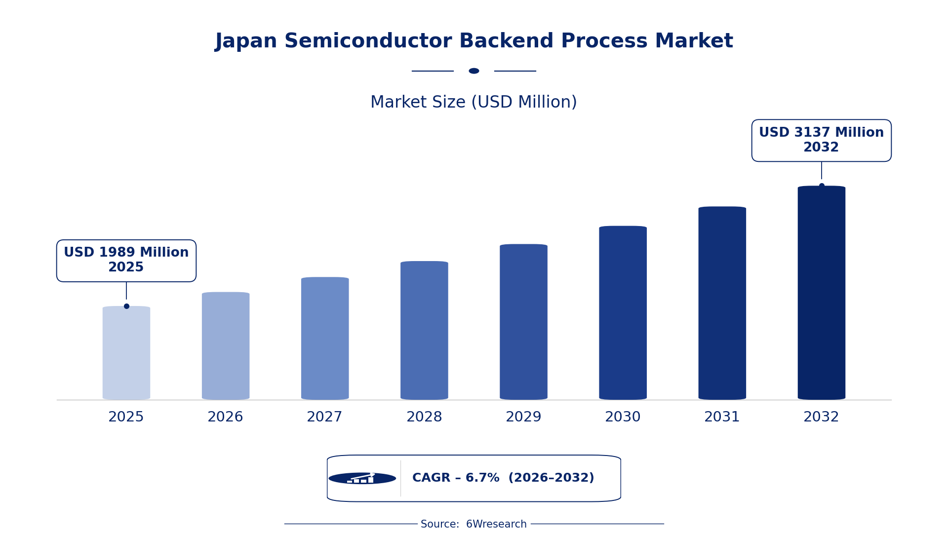
According to 6Wresearch internal database and industry insights, the Japan Semiconductor Backend Process Market was valued at USD 1,989 Million in 2025 and is projected to reach USD 3,137 Million by 2032, growing at a CAGR of approximately 6.7% during 2026–2032.
Japan Semiconductor Backend Process Market Highlights
| Report Metric | Details |
| Report Name | Japan Semiconductor Backend Process Market (2026-2032) |
| Market Size 2025 | USD 1,989 Million |
| Market Size 2032 | USD 3,137 Million |
| Absolute Growth 2025–2032 | USD 1,148 Million |
| CAGR 2026–2032 | 6.7% |
| Peak Annual Growth | 7.7% in 2029 |
| Forecast Period | 2026–2032 |
| Historical Data | 2022–2025 |
| Base Year | 2025 |
| Leading Process Type, 2025 | Wafer Dicing (42% share) |
| Leading Equipment Used, 2025 | Bonding Equipment (39% share) |
| Leading Output Function, 2025 | Electrical Interconnect (46% share) |
| Leading End User, 2025 | Foundries (46% share) |
| Fastest-Growing Process Type | Encapsulation (9.4% CAGR) |
| Fastest-Growing Equipment Used | Molding/Sealing Systems (9.2% CAGR) |
| Fastest-Growing Output Function | Chip Protection (9.1% CAGR) |
| Fastest-Growing End User | OSAT Providers (8.7% CAGR) |
| Growing Sector | OSAT Providers |
| Key End Users | Foundries, OSAT Providers, IDMs, IC Package Assemblers |
Japan Semiconductor Backend Process Market Year-wise Growth Rate and Key Drivers (2022–2032)
This graph illustrates the annual growth rates of the market from 2022 to 2032, highlighting a steady upward trajectory and projected market expansion over the forecast period.
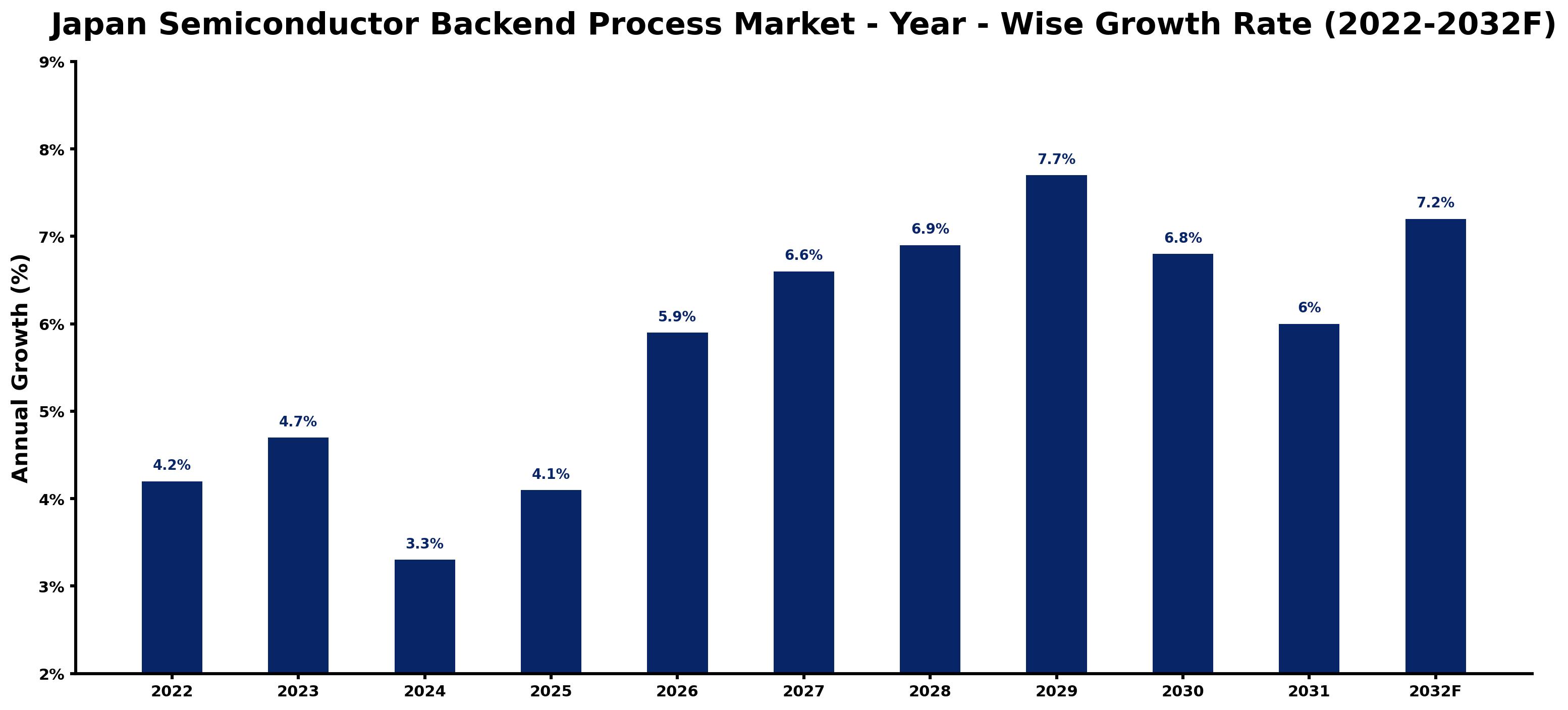
The yearly estimates that follow link every growth rate to its principal driver, so readers can see why the pace changed in each period.
| Year | Estimated Annual Growth (%) | Market Rationale |
| 2022 | 4.2 | The semiconductor market showed solid growth due to steady demand from consumer electronics. |
| 2023 | 4.7 | Production ramped up to meet rising automotive semiconductor needs, accelerating growth. |
| 2024 | 3.3 | A slowdown occurred as supply chain adjustments impacted production rates. |
| 2025 | 4.1 | Growth resumed as investments in semiconductor manufacturing began to pay off. |
| 2026 | 5.9 | Demand is expected to rise with new technology adoption in electronics. |
| 2027 | 6.6 | Projected increases in production capacity will drive further growth. |
| 2028 | 6.9 | Consumer electronics demand is anticipated to keep the market growing. |
| 2029 | 7.7 | Peak growth is expected as major production initiatives are implemented. |
| 2030 | 6.8 | Growth is set to slow as market saturation begins in some segments. |
| 2031 | 6.0 | Competitive pressures are expected to create a further slowdown in growth. |
| 2032 | 7.2 | Growth is expected to pick up again as new applications emerge. |
Note: Market size estimations and growth projections presented in this report are based on 6Wresearch's proprietary forecasting methodology, utilizing the latest available industry data, government publications, and primary research inputs.
Japan Semiconductor Backend Process Market Synopsis
The Semiconductor Backend Process involves technologies such as wafer dicing, die bonding, and encapsulation, essential for assembling integrated circuits. Japan Semiconductor Backend Process Market is valued at approximately $30 billion, driven by strong demand from consumer electronics and automotive sectors. Factors such as a projected 5% annual growth rate until 2025 and a $1 billion initiative to boost production are propelling this market forward, highlighting ongoing investments in semiconductor technology and infrastructure.
Market Dynamics Impact Analysis (2026–2032)
| Factor | Type | Impact | Primary Segment Affected |
| Growing demand for automotive semiconductors | Driver | High | Die Bonding |
| Investment in semiconductor manufacturing facilities | Driver | High | Wafer Dicing |
| Emerging demand for advanced packaging solutions | Opportunity | High | Encapsulation |
| Increased exports to meet global demand | Opportunity | Medium | Wire Bonding |
| Supply chain disruptions affecting production | Restraint | High | Bonding Equipment |
| High operational costs for semiconductor manufacturing | Restraint | Medium | Electrical Interconnect |
| Technological advancements requiring continuous investment | Challenge | High | Chip Protection |
| Intense competition from global semiconductor markets | Challenge | Medium | Foundries |
Evaluation of Drivers in Japan Semiconductor Backend Process Market (2026–2032)
These are the developments adding the most demand over the forecast period.
| Drivers | Primary Segment Affected | Why It Matters (Evidence) |
| Rising automotive production | Die Bonding | Increased vehicle manufacturing, particularly electric vehicles, drives demand for die bonding processes, which improves production efficiency. |
| Investment in new facilities | Wafer Dicing | The establishment of advanced semiconductor facilities in regions like Tokyo boosts demand for wafer dicing technologies. |
| Growing consumer electronics market | Encapsulation | The demand for reliable semiconductor packaging in consumer electronics is increasing, leading to higher encapsulation needs. |
| Technological advancements in semiconductor design | Wire Bonding | Innovations in chip design necessitate advanced wire bonding techniques to ensure connectivity and performance. |
| Export growth in semiconductor products | Bonding Equipment | Japan's semiconductor exports reached $15 billion in 2022, increasing the need for efficient bonding equipment. |
Orders keep climbing as the automotive sector expands, with vehicle production rising significantly. In 2022, Japan produced 1.5 million semiconductor wafers, reflecting the need for advanced manufacturing processes. Investments in new facilities, particularly in Tokyo and Osaka, are expected to drive demand for wafer dicing technologies. The consumer electronics market, valued at approximately $30 billion, further fuels the need for encapsulation. In addition, Japan's semiconductor exports reached $15 billion in 2022, increasing the demand for bonding equipment.
Evaluation of Restraints in Japan Semiconductor Backend Process Market
The main factors holding the market back are set out below.
| Market Restraint | Primary Segment Affected | Why It Matters (Evidence) |
| Stringent regulatory requirements | Die Bonding | Compliance costs for producers increase, delaying project timelines by up to six months. |
| Skills gap in advanced semiconductor technologies | Encapsulation | This leads to inefficiencies that cost producers approximately $2 billion annually in lost productivity. |
| Supply chain disruptions | Wafer Dicing | Sourcing critical materials can extend lead times for importers by 20%, impacting timely delivery. |
| Rapid technological advancements | Wire Bonding | Constant investment strains budgets for producers, limiting their capacity to innovate and compete. |
| Market saturation in some segments | Bonding Equipment | This can lead to reduced demand for certain products, affecting overall sales. |
Japan Semiconductor Backend Process Market Challenges
Japan's semiconductor backend process faces strict regulatory standards that raise compliance costs for producers, delaying projects by up to six months. A shortage of skilled workers in advanced semiconductor technologies leads to inefficiencies, costing producers approximately $2 billion each year in lost productivity. Supply chain disruptions, particularly in sourcing essential materials, can extend lead times for distributors by 20%, hindering their ability to fulfil buyer demands on time. Rapid technological changes require ongoing investments, straining budgets for producers and limiting their capacity to innovate and remain competitive.
Trends in the Japan Semiconductor Backend Process Market
Four trends stand out in the Japan Semiconductor Backend Process Market.
- Shift Towards Automation in Semiconductor Manufacturing: The introduction of automated systems in wafer dicing processes is reshaping production efficiency. In 2022, Japan produced 1.5 million semiconductor wafers, highlighting the need for advanced automation.
- Emergence of Advanced Packaging Techniques: In 2023, the adoption of new encapsulation methods is gaining traction among semiconductor manufacturers. This shift is driven by the demand for improved reliability in electronic devices.
- Increased Focus on Sustainability in Production: The Green Growth Strategy aims to reduce carbon emissions in semiconductor manufacturing by 2030. This initiative is prompting investments in eco-friendly technologies.
- Expansion of OSAT Providers in the Market: The OSAT Providers segment is expected to grow as demand for outsourced assembly services increases. This trend is projected to reach an 8.7% CAGR by 2032.
Investment Opportunities in the Japan Semiconductor Backend Process Market
The opportunities below stand out in the Japan Semiconductor Backend Process Market for new entrants and existing suppliers.
- Foundries Seeking Advanced Equipment: Foundries are increasingly looking for new bonding equipment to improve production efficiency. With Japan's semiconductor market valued at $30 billion, this presents a substantial investment opportunity.
- Supply of Molding/Sealing Systems: The growing need for reliable encapsulation solutions opens avenues for suppliers of molding and sealing systems. This is particularly relevant as Japan's semiconductor exports reached $15 billion in 2022.
- Investment in Semiconductor Facilities in Osaka: The Osaka region is set for growth as new semiconductor facilities are established. This presents opportunities for local partnerships to meet the rising demand.
- Gap in Skilled Workforce for Semiconductor Technologies: With a projected skills gap costing producers $2 billion annually, training programs for semiconductor technologies represent a critical investment opportunity.
Government Initiatives in the Japan Semiconductor Backend Process Market
The Semiconductor and Digital Industry Strategy, established by METI in June 2021, aims to secure domestic semiconductor manufacturing through various support measures. This includes funding for research and development to improve production capabilities and boost competitiveness in the global market.
In 2023, Japan allocated $1 billion to increase semiconductor production, administered by the Ministry of Economy, Trade and Industry (METI). This funding supports the development of advanced manufacturing technologies and infrastructure, directly benefiting semiconductor backend processes.
Future Insight of the Japan Semiconductor Backend Process Market
The launch of new semiconductor fabrication facilities will improve production capabilities and address rising demand. By 2032, Japan's semiconductor exports are expected to reach $20 billion, driven by enhancements in automation and precision engineering. The widespread adoption of the ISO 9001 standard will ensure consistent quality across processes. Partnerships with educational institutions will equip the workforce with essential skills to meet future industry requirements.
Market Segmentation Analysis
Japan Semiconductor Backend Process Market report covers a detailed analysis of the following market segments:
By Process Type – Wafer Dicing Leads, Encapsulation Expected to Grow Fastest
According to Saurav Kr Singh, Senior Research Analyst at 6Wresearch, with 42% of process type revenue in 2025, Wafer Dicing was the largest category. Wafer dicing holds the largest share due to its critical role in separating individual chips from wafers, essential for integrated circuit production. The substantial output of 1.5 million semiconductor wafers in Japan in 2022 highlights the ongoing necessity of this process. Encapsulation is projected to grow fastest, at a CAGR of 9.4% during 2026–2032. Encapsulation is experiencing rapid growth as it is vital for protecting semiconductor devices from environmental damage, particularly in consumer electronics. The projected average annual growth rate of semiconductor demand in Japan at 5% until 2025 will further enhance this segment's importance. Suppliers should prioritise advancements in encapsulation technologies to meet the increasing demand from manufacturers.
By Equipment Used – Bonding Equipment Leads, Molding/Sealing Systems Expected to Grow Fastest
Bonding Equipment held 39% of the Japan Semiconductor Backend Process Market by equipment used in 2025. Bonding equipment is the leading segment, integral for die bonding in semiconductor assembly, ensuring the reliability of final products. The existence of over 50 operational semiconductor foundries in Japan underscores the high demand for this essential equipment. Over 2026–2032, Molding/Sealing Systems are expected to post the fastest growth, at a CAGR of 9.2%. Molding/sealing systems are the fastest-growing equipment type, crucial for encapsulating semiconductor packages and protecting chips. The recent $1 billion initiative to boost semiconductor production in Japan will likely accelerate the adoption of these systems. Buyers should invest in advanced molding/sealing systems to enhance their production capabilities.
By Output Function – Electrical Interconnect Leads, Chip Protection Expected to Grow Fastest
In 2025, Electrical Interconnect led the output function split with a 46% share. Electrical interconnect is the dominant output function, essential for ensuring connectivity in semiconductor devices, which is fundamental for their overall performance. Its extensive application across various electronic devices solidifies its strong market position. The quickest growth will come from Chip Protection, forecast to expand at a CAGR of 9.1% between 2026 and 2032. Chip protection is the fastest-growing output function, necessary for safeguarding chips from physical damage, particularly in high-demand sectors like automotive. The increasing complexity of electronic devices will drive the need for enhanced protection solutions. Manufacturers must focus on innovations in chip protection to stay competitive in the evolving market.
By End User – Foundries Lead, OSAT Providers Expected to Grow Fastest
Foundries accounted for 46% of the market by end user in 2025. Foundries are the primary users of backend processes for chip manufacturing, making them the largest segment in the market. Their critical role in producing semiconductor wafers and components ensures a steady demand for backend services. OSAT Providers are set to record the highest CAGR in this split, 8.7% over 2026–2032. OSAT providers are the fastest-growing end user group, as they increasingly outsource semiconductor assembly and test services to meet the rising demand for packaged chips. The growth in Japan's semiconductor exports, reaching $15 billion in 2022, supports this trend. Suppliers should consider partnerships with OSAT providers to expand their market reach.
Key Attractiveness of the Report
- 10 Years of Market Numbers
- Historical Data Starting from 2022 to 2025
- Base Year 2025
- Forecast Data until 2032
- Key Performance Indicators Impacting the Market
- Major Upcoming Developments and Projects
Key Highlights of the Report:
- Japan Semiconductor Backend Process Market Outlook
- Market Size of Japan Semiconductor Backend Process Market, 2025
- Forecast of Japan Semiconductor Backend Process Market, 2032
- Historical Data and Forecast of Japan Semiconductor Backend Process Revenues & Volume for the Period 2022-2032F
- Japan Semiconductor Backend Process Market Trend Evolution
- Japan Semiconductor Backend Process Market Drivers and Challenges
- Japan Semiconductor Backend Process Price Trends
- Japan Semiconductor Backend Process Porter's Five Forces
- Japan Semiconductor Backend Process Industry Life Cycle
- Historical Data and Forecast of Japan Semiconductor Backend Process Market Revenues & Volume By Process Type for the Period 2022-2032F
- Historical Data and Forecast of Japan Semiconductor Backend Process Market Revenues & Volume By Wafer Dicing for the Period 2022-2032F
- Historical Data and Forecast of Japan Semiconductor Backend Process Market Revenues & Volume By Die Bonding for the Period 2022-2032F
- Historical Data and Forecast of Japan Semiconductor Backend Process Market Revenues & Volume By Wire Bonding for the Period 2022-2032F
- Historical Data and Forecast of Japan Semiconductor Backend Process Market Revenues & Volume By Encapsulation for the Period 2022-2032F
- Historical Data and Forecast of Japan Semiconductor Backend Process Market Revenues & Volume By Equipment Used for the Period 2022-2032F
- Historical Data and Forecast of Japan Semiconductor Backend Process Market Revenues & Volume By Laser/Cutting Tools for the Period 2022-2032F
- Historical Data and Forecast of Japan Semiconductor Backend Process Market Revenues & Volume By Bonding Equipment for the Period 2022-2032F
- Historical Data and Forecast of Japan Semiconductor Backend Process Market Revenues & Volume By Gold/Aluminum Wires for the Period 2022-2032F
- Historical Data and Forecast of Japan Semiconductor Backend Process Market Revenues & Volume By Molding/Sealing Systems for the Period 2022-2032F
- Historical Data and Forecast of Japan Semiconductor Backend Process Market Revenues & Volume By Output Function for the Period 2022-2032F
- Historical Data and Forecast of Japan Semiconductor Backend Process Market Revenues & Volume By Wafer Segmentation for the Period 2022-2032F
- Historical Data and Forecast of Japan Semiconductor Backend Process Market Revenues & Volume By Die Placement for the Period 2022-2032F
- Historical Data and Forecast of Japan Semiconductor Backend Process Market Revenues & Volume By Electrical Interconnect for the Period 2022-2032F
- Historical Data and Forecast of Japan Semiconductor Backend Process Market Revenues & Volume By Chip Protection for the Period 2022-2032F
- Historical Data and Forecast of Japan Semiconductor Backend Process Market Revenues & Volume By End User for the Period 2022-2032F
- Historical Data and Forecast of Japan Semiconductor Backend Process Market Revenues & Volume By Foundries for the Period 2022-2032F
- Historical Data and Forecast of Japan Semiconductor Backend Process Market Revenues & Volume By OSAT Providers for the Period 2022-2032F
- Historical Data and Forecast of Japan Semiconductor Backend Process Market Revenues & Volume By IC Package Assemblers for the Period 2022-2032F
- Historical Data and Forecast of Japan Semiconductor Backend Process Market Revenues & Volume By IDMs for the Period 2022-2032F
- Japan Semiconductor Backend Process Import Export Trade Statistics
- Market Opportunity Assessment By Process Type
- Market Opportunity Assessment By Equipment Used
- Market Opportunity Assessment By Output Function
- Market Opportunity Assessment By End User
- Japan Semiconductor Backend Process Top Companies Market Share
- Japan Semiconductor Backend Process Competitive Benchmarking By Technical and Operational Parameters
- Japan Semiconductor Backend Process Company Profiles
- Japan Semiconductor Backend Process Key Strategic Recommendations
Market Covered
The study includes the following segmentation.
By Process Type
- Wafer Dicing
- Die Bonding
- Wire Bonding
- Encapsulation
By Equipment Used
- Laser/Cutting Tools
- Bonding Equipment
- Gold/Aluminum Wires
- Molding/Sealing Systems
By Output Function
- Wafer Segmentation
- Die Placement
- Electrical Interconnect
- Chip Protection
By End User
- Foundries
- OSAT Providers
- IC Package Assemblers
- IDMs