Japan Semiconductor Inspection Market Size & Growth Rate
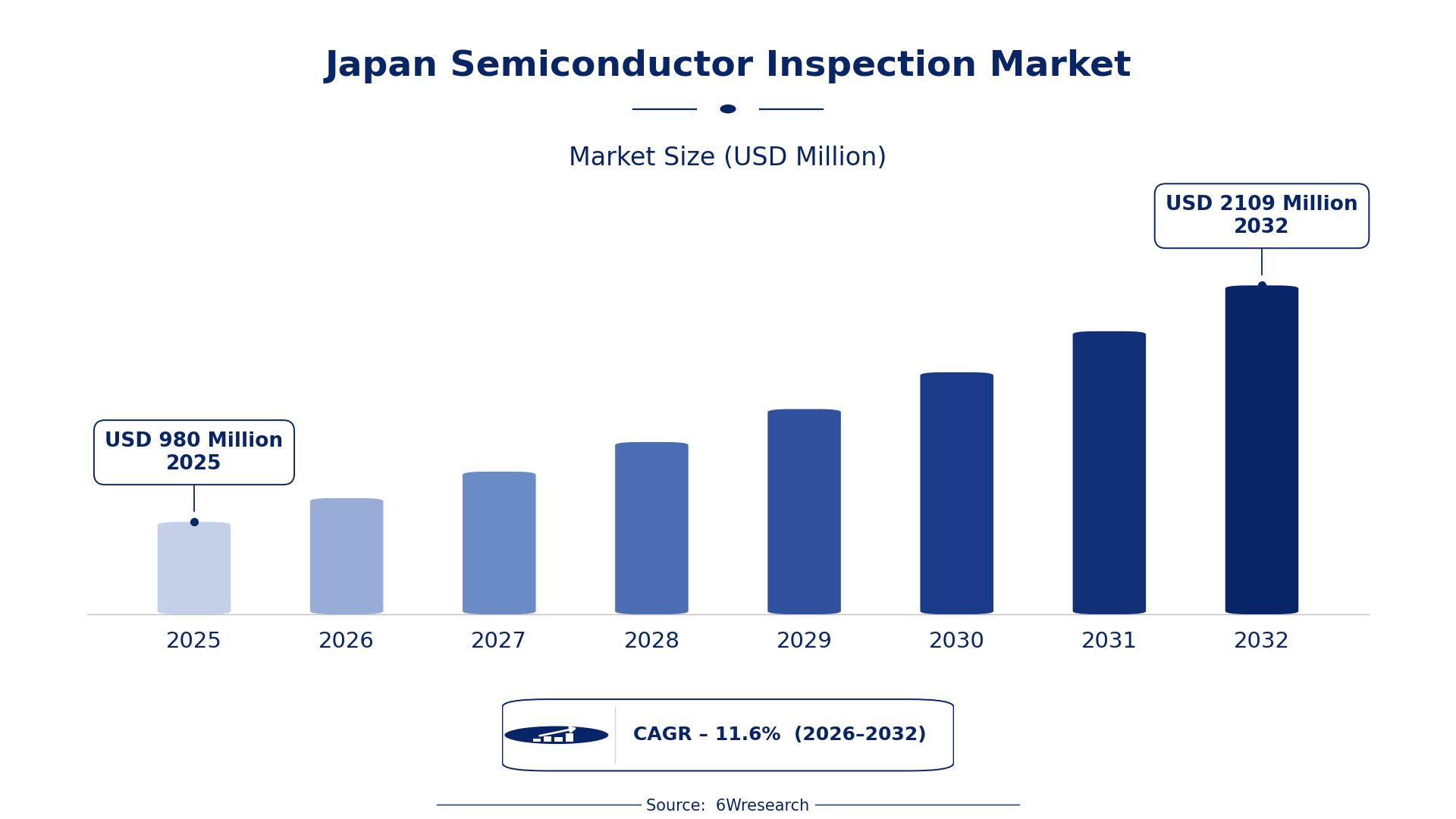
According to 6Wresearch internal database and industry insights, the Japan Semiconductor Inspection Market was valued at USD 980 Million in 2025 and is projected to reach USD 2,109 Million by 2032, growing at a CAGR of approximately 11.6% during 2026–2032.
Japan Semiconductor Inspection Market Highlights
| Report Metric | Details |
| Report Name | Japan Semiconductor Inspection Market (2026-2032) |
| Market Size 2025 | USD 980 Million |
| Market Size 2032 | USD 2,109 Million |
| Absolute Growth 2025–2032 | USD 1,129 Million |
| CAGR 2026–2032 | 11.6% |
| Peak Annual Growth | 12.5% in 2028 |
| Forecast Period | 2026–2032 |
| Historical Data | 2022–2025 |
| Base Year | 2025 |
| Leading Inspection Type, 2025 | Wafer Inspection (44% share) |
| Leading Stage of Inspection, 2025 | Post-Deposition (40% share) |
| Leading Technology Used, 2025 | Optical + e-Beam (47% share) |
| Leading End User, 2025 | Foundries & IDMs (37% share) |
| Fastest-Growing Inspection Type | Die Inspection (15.8% CAGR) |
| Fastest-Growing Stage of Inspection | Pre-Packaging (16.2% CAGR) |
| Fastest-Growing Technology Used | SEM/X-ray (16.9% CAGR) |
| Fastest-Growing End User | OSATs (15.6% CAGR) |
| Growing Sector | OSATs |
| Key End Users | Foundries & IDMs, OSATs, Photomask Makers, Advanced Node Fabs |
Japan Semiconductor Inspection Market Year-wise Growth Rate and Key Drivers (2022–2032)
This graph illustrates the annual growth rates of the market from 2022 to 2032, highlighting a steady upward trajectory and projected market expansion over the forecast period.
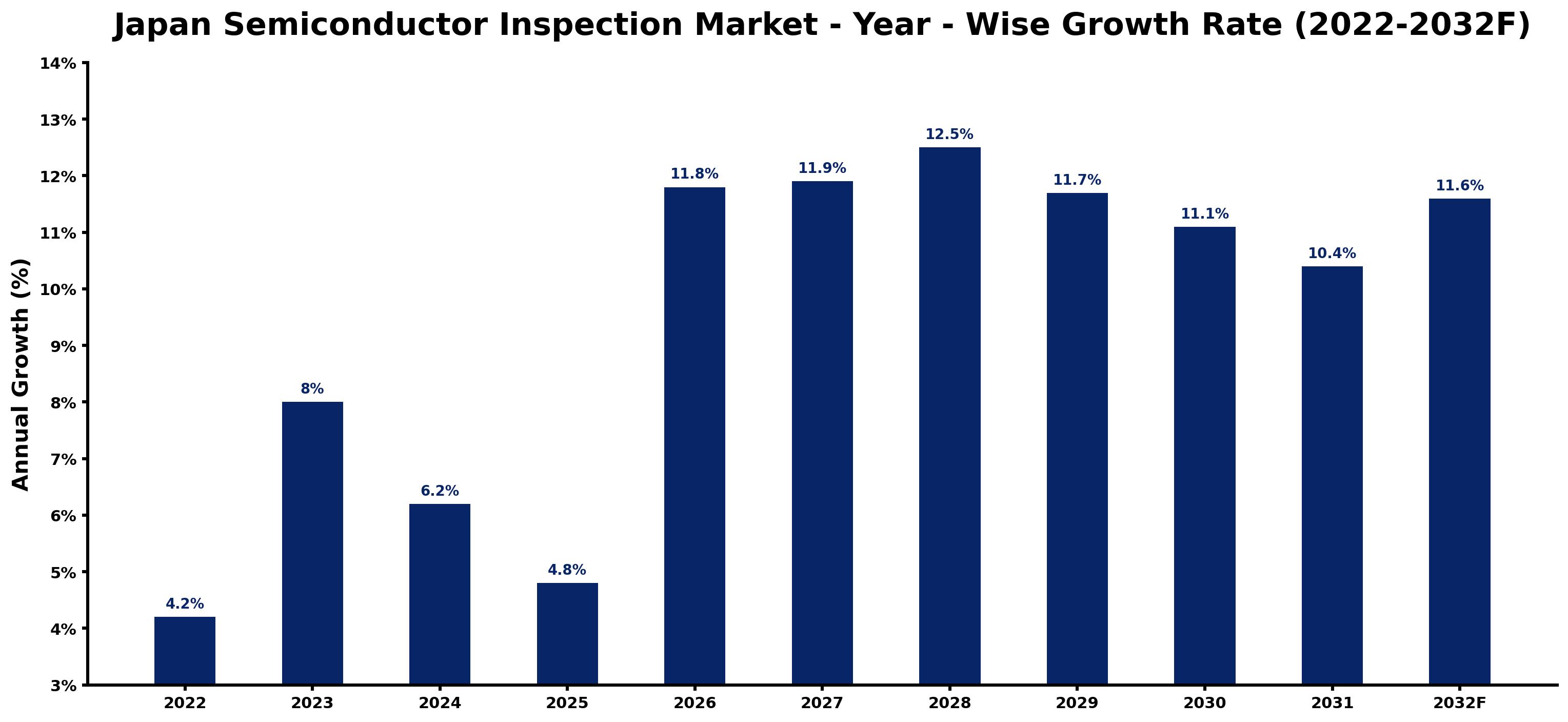
For each year, the table pairs the estimated growth rate with the leading influence on demand, showing how the drivers changed across the period.
| Year | Estimated Annual Growth (%) | Market Rationale |
| 2022 | 4.2 | The market showed steady growth due to ongoing investments in semiconductor technology. |
| 2023 | 8.0 | Growth accelerated as demand surged from domestic foundries and advanced node fabs. |
| 2024 | 6.2 | Market growth slowed as companies adjusted to supply chain challenges and production fluctuations. |
| 2025 | 4.8 | Demand continued to rise, albeit at a slower pace, as manufacturers focused on quality control. |
| 2026 | 11.8 | Growth is expected to increase due to new funding for semiconductor R&D initiatives. |
| 2027 | 11.9 | The market will maintain momentum, driven by advancements in inspection technology. |
| 2028 | 12.5 | A peak in growth will occur as demand for high-precision inspection systems surges. |
| 2029 | 11.7 | Growth rate will slow slightly as the market begins to stabilise after the peak. |
| 2030 | 11.1 | Continued demand for inspection systems will support steady growth, albeit at a reduced rate. |
| 2031 | 10.4 | The market will experience a further slowdown as saturation in certain segments begins to occur. |
| 2032 | 11.6 | Growth is expected to rise again as new technologies and applications emerge. |
Note: Market size estimations and growth projections presented in this report are based on 6Wresearch's proprietary forecasting methodology, utilizing the latest available industry data, government publications, and primary research inputs.
Japan Semiconductor Inspection Market Synopsis
Semiconductor inspection utilises advanced technologies to detect defects and ensure the quality of semiconductor wafers and components. The Japan Semiconductor Inspection Market is expanding due to rising demand from domestic foundries and advanced node fabs, along with substantial investments in R&D, such as the Semiconductor and Digital Industry Strategy. With the annual demand for semiconductor inspection systems projected to reach around 100 billion yen by 2025, the market is well-positioned for growth as it adapts to evolving technological needs.
Market Dynamics Impact Analysis (2026–2032)
| Factor | Type | Impact | Primary Segment Affected |
| Increasing demand for high-quality semiconductor products | Driver | High | Wafer Inspection |
| Technological advancements in inspection methods | Driver | High | Die Inspection |
| Growing investments in semiconductor R&D | Opportunity | High | Post-Deposition |
| Expansion of semiconductor manufacturing facilities | Opportunity | High | Foundries & IDMs |
| Limited availability of skilled workforce | Restraint | High | OSATs |
| High costs associated with advanced inspection systems | Restraint | Medium | Mask Inspection |
| Supply chain disruptions affecting equipment availability | Challenge | High | Defect Review Systems |
| Rapid technological changes requiring constant upgrades | Challenge | Medium | Pre-Packaging |
Evaluation of Drivers in Japan Semiconductor Inspection Market (2026–2032)
The following drivers explain most of the expected growth.
| Drivers | Primary Segment Affected | Why It Matters (Evidence) |
| Rising demand for high-quality semiconductor products | Die Inspection | This trend leads foundries to invest in advanced inspection systems, enhancing defect detection and yield rates. |
| Increased investments in semiconductor R&D | Wafer Inspection | Funding boosts the development of cutting-edge inspection technologies, driving manufacturers to upgrade their systems. |
| Expansion of semiconductor manufacturing facilities | Post-Deposition | New fabs require advanced quality control measures, resulting in higher purchases of inspection systems. |
| Adoption of advanced standards like ISO 9001 | Mask Inspection | Compliance drives manufacturers to enhance their inspection processes, ensuring quality assurance in production. |
| Collaboration among industry players | Defect Review Systems | Joint efforts improve technology sharing and innovation, increasing the efficiency of inspection systems. |
Several shifts outside the market lift sales. The demand for high-quality semiconductor products has led to a surge in investments in inspection systems, with the annual demand projected to reach around 100 billion yen by 2025. New advancements in die inspection methods improve defect detection capabilities, prompting foundries to adopt these systems for better yield. Increased investments in semiconductor R&D drive manufacturers to upgrade their inspection equipment. The expansion of semiconductor manufacturing facilities also contributes to higher purchases of inspection systems, as new fabs require advanced quality control measures.
Evaluation of Restraints in Japan Semiconductor Inspection Market
The key brakes on demand, and where they bite hardest, are shown below.
| Market Restraint | Primary Segment Affected | Why It Matters (Evidence) |
| Limited availability of skilled workforce | OSATs | The shortage of qualified personnel in the semiconductor industry hampers OSATs' ability to implement advanced inspection technologies. |
| High costs associated with advanced inspection systems | Mask Inspection | The substantial investment required for advanced inspection technologies can deter smaller manufacturers from upgrading their equipment. |
| Supply chain disruptions affecting equipment availability | Defect Review Systems | Ongoing supply chain issues delay the procurement of essential inspection equipment, impacting production timelines. |
| Rapid technological changes requiring constant upgrades | Pre-Packaging | The fast pace of technological advancements necessitates frequent updates to inspection systems, increasing operational costs for manufacturers. |
| Regulatory compliance challenges | Post-Deposition | Meeting stringent quality standards complicates the inspection process, leading to potential delays and increased costs. |
Japan Semiconductor Inspection Market Challenges
Buyers face supply issues as many rely on imported inspection equipment, potentially delaying production timelines by up to six months. Suppliers encounter rising costs from fluctuating material prices, which could increase prices by 15% for buyers. Technology gaps persist, as many semiconductor fabs do not possess the latest inspection systems, resulting in a 20% decline in quality assurance efficiency for producers. Compliance with ISO 9001 can prolong the certification process, causing delays of up to three months for suppliers striving to meet industry standards.
Trends in the Japan Semiconductor Inspection Market
The following changes are redrawing the Japan Semiconductor Inspection Market.
- Shift towards Automation in Semiconductor Inspection: Japan's semiconductor industry is increasingly embracing automated inspection systems to boost efficiency and accuracy. The integration of AI and machine vision technologies is expected to grow, with investments projected at 15 billion yen by 2025.
- Transition from Optical to Electron Beam Inspection: The market is moving away from traditional optical methods towards electron beam inspection for enhanced precision. This shift is particularly noticeable in advanced node fabs, where demand for electron beam systems is anticipated to rise significantly.
- Emergence of AI-Driven Inspection Technologies: AI-driven inspection technologies are gaining traction, especially in Tokyo's semiconductor fabs. With an estimated growth rate of 18% in AI applications, manufacturers are increasingly adopting these technologies to refine defect detection.
- Focus on Environmental Sustainability in Manufacturing: There is a growing emphasis on sustainable practices within Japan's semiconductor industry, motivated by the Green Growth Strategy. By 2025, investments in green technologies are expected to reach 30 billion yen, promoting eco-friendly inspection methods.
Investment Opportunities in the Japan Semiconductor Inspection Market
Several openings in the Japan Semiconductor Inspection Market merit attention from investors.
- Collaboration with Local Manufacturers: Forming joint ventures with local manufacturers can ease entry into the Japanese semiconductor inspection market. With an annual demand of around 100 billion yen by 2025, this presents a timely opportunity for investment.
- Expansion into Advanced Node Fabs: The demand for advanced inspection systems is increasing, particularly in advanced node fabs. Investing in high-precision inspection technologies can serve this expanding market segment, which is projected to grow significantly.
- Investment in Training Programs: There is a pressing need for skilled personnel in the semiconductor inspection sector. Establishing training programs can fill this gap, ensuring a steady supply of qualified workers to meet industry demands.
- Development of Eco-Friendly Inspection Solutions: With sustainability in focus, there is an opportunity to create eco-friendly inspection solutions. The Green Growth Strategy is driving investments in green technologies, establishing a market for progressive inspection methods.
Government Initiatives in the Japan Semiconductor Inspection Market
The Semiconductor and Digital Industry Strategy, established in June 2021, outlines measures to strengthen Japan's semiconductor manufacturing capabilities. This law aims to enhance the industry's capacity and competitiveness, ensuring that Japan remains a key player in the global semiconductor market. The Economic Security Promotion Act, introduced in 2022, supports supply-chain resilience for designated critical products and materials, which includes semiconductor inspection technologies.
Manufacturers in the semiconductor sector benefit from initiatives aimed at increasing R&D funding by 20% annually until 2025. This program encourages innovation and assists manufacturers in upgrading their inspection systems to meet evolving standards. The Japan Electronics and Information Technology Industries Association also plays a role in promoting semiconductor innovation and collaboration across the industry.
Future Insight of the Japan Semiconductor Inspection Market
Domestic foundries will gain from the Advanced Semiconductor Manufacturing Program, which boosts R&D funding and drives innovation in inspection technologies. By 2032, the annual demand for semiconductor inspection systems is projected to reach 100 billion yen, reflecting the growing need for quality assurance. The Semiconductor Manufacturing Equipment Standard will streamline processes, enabling suppliers to align more effectively with buyer needs. Collaboration encouraged by the Japan Semiconductor Manufacturing Association will strengthen industry standards and enhance overall market efficiency.
Market Segmentation Analysis
Japan Semiconductor Inspection Market report covers a detailed analysis of the following market segments:
By Inspection Type – Wafer Inspection Leads, Die Inspection Expected to Grow Fastest
According to Saurav Kr Singh, Senior Research Analyst at 6Wresearch, Wafer Inspection took 44% of inspection type revenue in 2025, more than any other category. Wafer inspection holds the largest share due to its critical role in quality control during semiconductor manufacturing, particularly in advanced node fabs. The installed base of approximately 1,200 units in Japan highlights its widespread use among domestic foundries. Die Inspection is set to record the highest CAGR in this split, 15.8% over 2026–2032. Die inspection is experiencing rapid growth as it is vital for ensuring die integrity and performance, particularly with the increasing demand for high-quality semiconductor components. This growth is reflected in the projected annual demand for semiconductor inspection systems, expected to reach 100 billion yen by 2025. Suppliers must focus on enhancing die inspection technologies to meet the rising needs of the semiconductor market.
By Stage of Inspection – Post-Deposition Leads, Pre-Packaging Expected to Grow Fastest
With 40% of stage of inspection revenue in 2025, Post-Deposition was the largest category. Post-deposition inspection leads the market as it is essential for identifying defects in layers after deposition, crucial for maintaining product quality. This stage is particularly important for advanced technologies, ensuring that defects are detected early in the manufacturing process. The quickest growth will come from Pre-Packaging, forecast to expand at a CAGR of 16.2% between 2026 and 2032. Pre-packaging inspection is the fastest-growing stage, as it plays a key role in quality assurance before packaging, which is increasingly important with the rise of compact electronic devices. The emphasis on quality control at this stage is expected to intensify alongside the growth of the semiconductor market. Buyers should invest in pre-packaging inspection solutions to ensure high-quality outputs in their semiconductor production.
By Technology Used – Optical + e-Beam Leads, SEM/X-ray Expected to Grow Fastest
The largest technology used category in 2025 was Optical + e-Beam, at 47% of revenue. The combination of optical and electron beam technologies dominates the market due to their effectiveness in high-resolution inspections, making them the preferred choice for semiconductor manufacturers. This technology is widely adopted across various inspection stages, ensuring quality throughout the production process. SEM/X-ray is projected to grow fastest, at a CAGR of 16.9% during 2026–2032. SEM/X-ray technology is growing rapidly as it is employed for detailed defect analysis, which is increasingly necessary with the complexity of modern semiconductor devices. The demand for precise defect detection is driving this segment's growth. Suppliers must invest in SEM/X-ray technologies to capitalise on the increasing need for detailed inspections in semiconductor manufacturing.
By End User – Foundries & IDMs Lead, OSATs Expected to Grow Fastest
Foundries & IDMs held 37% of the Japan Semiconductor Inspection Market by end user in 2025. Foundries and IDMs dominate the market as they are the primary users of inspection technologies, which are crucial for maintaining quality in semiconductor production. Their significant investment in quality control systems underscores the importance of these technologies in the supply chain. Over 2026–2032, OSATs are expected to post the fastest growth, at a CAGR of 15.6%. OSATs represent the fastest-growing end user segment, as they are integral to packaging and testing processes, which are essential for the semiconductor lifecycle. The increasing complexity of semiconductor packaging is a key factor driving this rapid growth. Suppliers should tailor their products to meet the specific requirements of OSATs to seize emerging market opportunities.
Key Attractiveness of the Report
- 10 Years of Market Numbers
- Historical Data Starting from 2022 to 2025
- Base Year 2025
- Forecast Data until 2032
- Key Performance Indicators Impacting the Market
- Major Upcoming Developments and Projects
Key Highlights of the Report:
- Japan Semiconductor Inspection Market Outlook
- Market Size of Japan Semiconductor Inspection Market, 2025
- Forecast of Japan Semiconductor Inspection Market, 2032
- Historical Data and Forecast of Japan Semiconductor Inspection Revenues & Volume for the Period 2022-2032F
- Japan Semiconductor Inspection Market Trend Evolution
- Japan Semiconductor Inspection Market Drivers and Challenges
- Japan Semiconductor Inspection Price Trends
- Japan Semiconductor Inspection Porter's Five Forces
- Japan Semiconductor Inspection Industry Life Cycle
- Historical Data and Forecast of Japan Semiconductor Inspection Market Revenues & Volume By Inspection Type for the Period 2022-2032F
- Historical Data and Forecast of Japan Semiconductor Inspection Market Revenues & Volume By Wafer Inspection for the Period 2022-2032F
- Historical Data and Forecast of Japan Semiconductor Inspection Market Revenues & Volume By Die Inspection for the Period 2022-2032F
- Historical Data and Forecast of Japan Semiconductor Inspection Market Revenues & Volume By Mask Inspection for the Period 2022-2032F
- Historical Data and Forecast of Japan Semiconductor Inspection Market Revenues & Volume By Defect Review Systems for the Period 2022-2032F
- Historical Data and Forecast of Japan Semiconductor Inspection Market Revenues & Volume By Stage of Inspection for the Period 2022-2032F
- Historical Data and Forecast of Japan Semiconductor Inspection Market Revenues & Volume By Post-Deposition for the Period 2022-2032F
- Historical Data and Forecast of Japan Semiconductor Inspection Market Revenues & Volume By Pre-Packaging for the Period 2022-2032F
- Historical Data and Forecast of Japan Semiconductor Inspection Market Revenues & Volume By Pre-Lithography for the Period 2022-2032F
- Historical Data and Forecast of Japan Semiconductor Inspection Market Revenues & Volume By Across Nodes for the Period 2022-2032F
- Historical Data and Forecast of Japan Semiconductor Inspection Market Revenues & Volume By Technology Used for the Period 2022-2032F
- Historical Data and Forecast of Japan Semiconductor Inspection Market Revenues & Volume By Optical + e-Beam for the Period 2022-2032F
- Historical Data and Forecast of Japan Semiconductor Inspection Market Revenues & Volume By SEM/X-ray for the Period 2022-2032F
- Historical Data and Forecast of Japan Semiconductor Inspection Market Revenues & Volume By UV Optical Scanning for the Period 2022-2032F
- Historical Data and Forecast of Japan Semiconductor Inspection Market Revenues & Volume By AI + Machine Vision for the Period 2022-2032F
- Historical Data and Forecast of Japan Semiconductor Inspection Market Revenues & Volume By End User for the Period 2022-2032F
- Historical Data and Forecast of Japan Semiconductor Inspection Market Revenues & Volume By Foundries & IDMs for the Period 2022-2032F
- Historical Data and Forecast of Japan Semiconductor Inspection Market Revenues & Volume By OSATs for the Period 2022-2032F
- Historical Data and Forecast of Japan Semiconductor Inspection Market Revenues & Volume By Photomask Makers for the Period 2022-2032F
- Historical Data and Forecast of Japan Semiconductor Inspection Market Revenues & Volume By Advanced Node Fabs for the Period 2022-2032F
- Japan Semiconductor Inspection Import Export Trade Statistics
- Market Opportunity Assessment By Inspection Type
- Market Opportunity Assessment By Stage of Inspection
- Market Opportunity Assessment By Technology Used
- Market Opportunity Assessment By End User
- Japan Semiconductor Inspection Top Companies Market Share
- Japan Semiconductor Inspection Competitive Benchmarking By Technical and Operational Parameters
- Japan Semiconductor Inspection Company Profiles
- Japan Semiconductor Inspection Key Strategic Recommendations
Market Covered
The study includes the following segmentation.
By Inspection Type
- Wafer Inspection
- Die Inspection
- Mask Inspection
- Defect Review Systems
By Stage of Inspection
- Post-Deposition
- Pre-Packaging
- Pre-Lithography
- Across Nodes
By Technology Used
- Optical + e-Beam
- SEM/X-ray
- UV Optical Scanning
- AI + Machine Vision
By End User
- Foundries & IDMs
- OSATs
- Photomask Makers
- Advanced Node Fabs