Japan Semiconductor Inspection Tools Market Size & Growth Rate
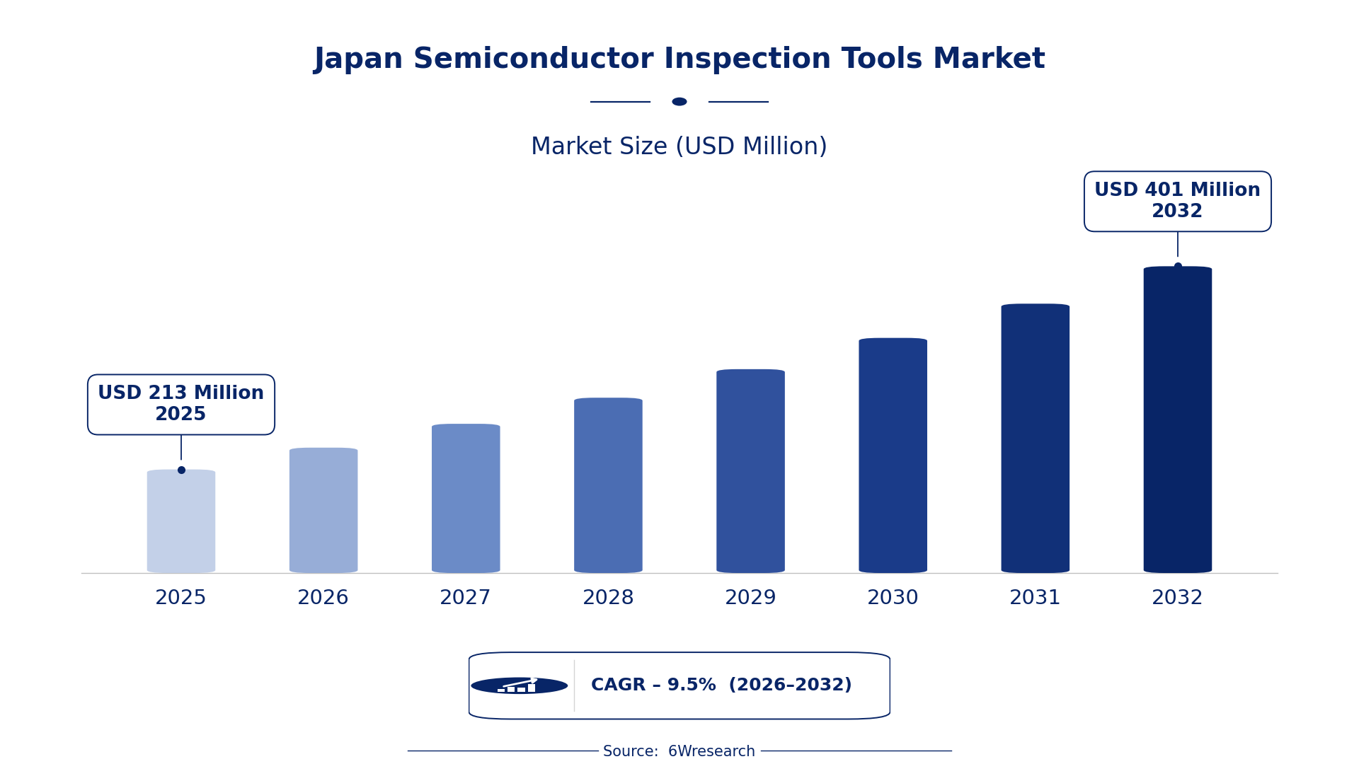
According to 6Wresearch internal database and industry insights, the Japan Semiconductor Inspection Tools Market was valued at USD 213 Million in 2025 and is projected to reach USD 401 Million by 2032, growing at a CAGR of approximately 9.5% during 2026–2032.
Japan Semiconductor Inspection Tools Market Highlights
| Report Metric | Details |
| Report Name | Japan Semiconductor Inspection Tools Market (2026-2032) |
| Market Size 2025 | USD 213 Million |
| Market Size 2032 | USD 401 Million |
| Absolute Growth 2025–2032 | USD 188 Million |
| CAGR 2026–2032 | 9.5% |
| Peak Annual Growth | 10.6% in 2028 |
| Forecast Period | 2026–2032 |
| Historical Data | 2022–2025 |
| Base Year | 2025 |
| Leading Tool Type, 2025 | Optical Inspection Tool (48% share) |
| Leading Functionality, 2025 | Surface Defect Detection (40% share) |
| Leading Automation Level, 2025 | Inline (57% share) |
| Leading End User, 2025 | Wafer Foundries (42% share) |
| Fastest-Growing Tool Type | E-Beam Tools (12.9% CAGR) |
| Fastest-Growing Functionality | Pattern Defect Analysis (12.1% CAGR) |
| Fastest-Growing Automation Level | Offline (12.4% CAGR) |
| Fastest-Growing End User | R&D Labs (12.0% CAGR) |
| Growing Sector | semiconductor manufacturing |
| Key End Users | wafer foundries, R&D labs, memory fabs, logic fabs |
Japan Semiconductor Inspection Tools Market Year-wise Growth Rate and Key Drivers (2022–2032)
This graph illustrates the annual growth rates of the market from 2022 to 2032, highlighting a steady upward trajectory and projected market expansion over the forecast period.
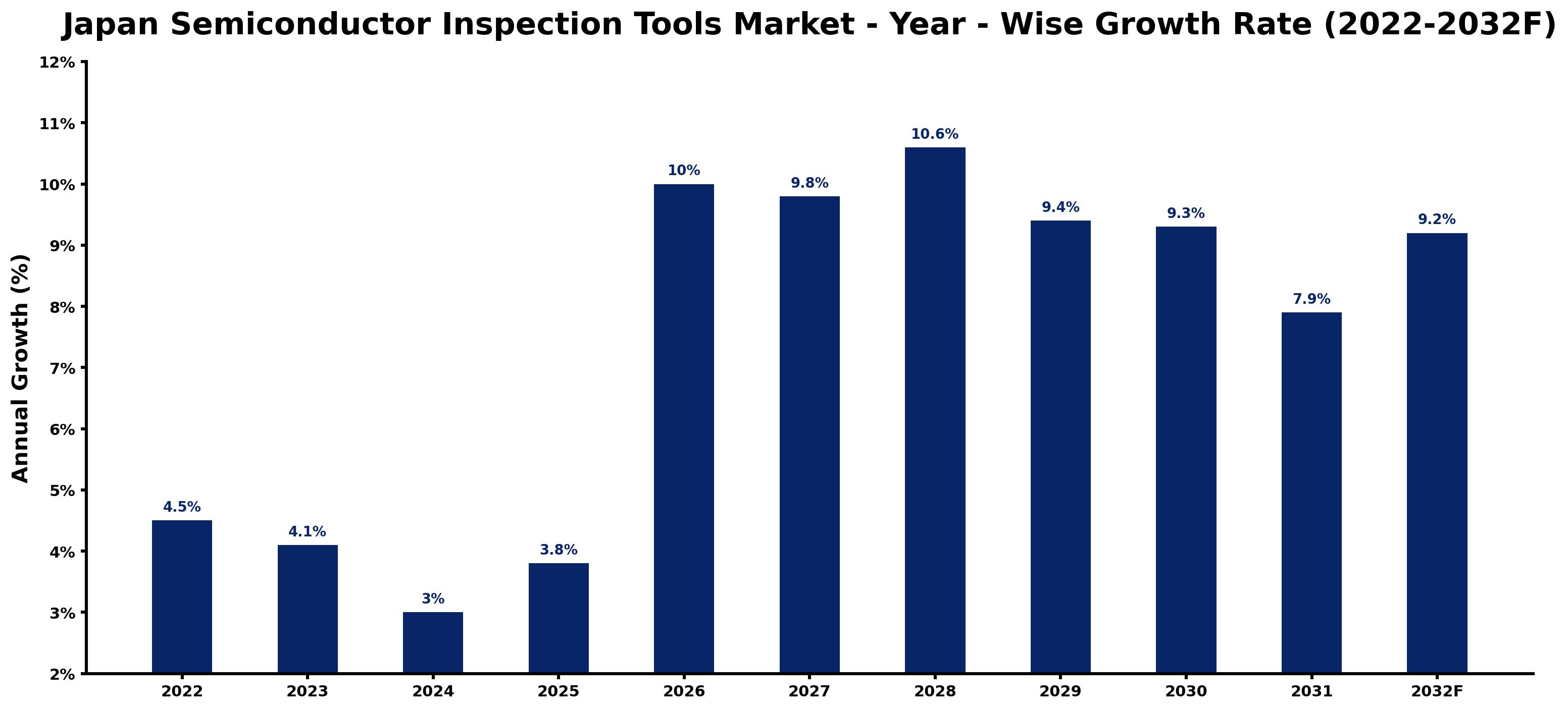
Each row of the following table gives one year's estimated growth and the event or demand shift that explains it.
| Year | Estimated Annual Growth (%) | Market Rationale |
| 2022 | 4.5 | The market experienced solid growth due to strong domestic demand from wafer foundries. |
| 2023 | 4.1 | Growth slowed slightly as companies adjusted to market conditions and supply chain challenges. |
| 2024 | 3.0 | Market growth continued to decelerate as manufacturers faced increasing operational costs. |
| 2025 | 3.8 | Demand picked up again as investments in advanced semiconductor technologies increased. |
| 2026 | 10.0 | Growth is expected to surge as the government initiates funding to improve semiconductor capabilities. |
| 2027 | 9.8 | The market will see a slight slowdown as companies consolidate their investments and strategies. |
| 2028 | 10.6 | Growth is projected to peak with rising demand for semiconductor inspection tools driven by AI applications. |
| 2029 | 9.4 | Market growth will slow as production capacities begin to stabilise across the industry. |
| 2030 | 9.3 | Demand is expected to continue slowing as companies focus on optimising existing technologies. |
| 2031 | 7.9 | The market will experience another slowdown as competition intensifies among suppliers. |
| 2032 | 9.2 | Growth is projected to rebound as new investments in semiconductor technologies revitalise demand. |
Note: Market size estimations and growth projections presented in this report are based on 6Wresearch's proprietary forecasting methodology, utilizing the latest available industry data, government publications, and primary research inputs.
Japan Semiconductor Inspection Tools Market Synopsis
Semiconductor inspection tools are crucial for identifying defects and measuring dimensions in semiconductor manufacturing. These sophisticated instruments are predominantly utilised by wafer foundries and research laboratories, ensuring the quality of semiconductor devices. The Japan Semiconductor Inspection Tools Market is growing due to increased domestic demand from local semiconductor firms, substantial investments in manufacturing capabilities, and an emphasis on advanced technologies such as AI and IoT applications. In 2022, the market was valued at approximately 4 trillion yen, highlighting its importance within the electronics sector.
Market Dynamics Impact Analysis (2026–2032)
| Factor | Type | Impact | Primary Segment Affected |
| Rising domestic demand from wafer foundries drives the need for advanced inspection tools. | Driver | High | Optical Inspection Tool |
| Increased investments in semiconductor manufacturing capabilities create opportunities for suppliers. | Driver | High | E-Beam Tools |
| Growing focus on AI and IoT applications enhances the demand for inspection tools. | Opportunity | High | CD-SEM Tools |
| R&D labs are expanding their capabilities, increasing demand for advanced inspection tools. | Opportunity | High | Metrology Tools |
| High operational costs can limit the adoption of advanced inspection technologies. | Restraint | Medium | Surface Defect Detection |
| Supply chain disruptions may hinder timely access to necessary components for production. | Restraint | Medium | Pattern Defect Analysis |
| Limited skilled workforce in semiconductor manufacturing affects production capacity. | Challenge | High | Critical Dimension Check |
| Intense competition among suppliers can lead to pricing pressures in the market. | Challenge | High | Film Thickness/Overlay |
Evaluation of Drivers in Japan Semiconductor Inspection Tools Market (2026–2032)
These are the developments adding the most demand over the forecast period.
| Drivers | Primary Segment Affected | Why It Matters (Evidence) |
| Increased domestic semiconductor production capacity boosts demand for inspection tools. | Optical Inspection Tool | The semiconductor market in Japan was valued at approximately 4 trillion yen in 2022. |
| Growing investments in semiconductor technology increase the need for advanced inspection solutions. | E-Beam Tools | Japan invested 1 trillion yen in 2023 to improve semiconductor manufacturing capabilities. |
| The rise of AI applications drives demand for precise semiconductor fabrication. | CD-SEM Tools | Japan's semiconductor market is expected to grow due to increased demand for AI applications. |
| Expansion of R&D labs increases the need for advanced measurement tools. | Metrology Tools | Over 400 semiconductor companies in Japan focus on R&D to improve production processes. |
| Demand for high-quality semiconductor products necessitates advanced inspection technologies. | Surface Defect Detection | The Japanese semiconductor industry employs around 100,000 people, highlighting its importance. |
Buyers are adding capacity as the semiconductor industry in Japan focuses on R&D, with over 400 companies driving innovation. In 2023, Japan's investment of 1 trillion yen to improve manufacturing capabilities supports this growth. The market is responding to rising interest in AI applications, which will boost production. The expansion of R&D labs further increases the need for advanced measurement tools, driving demand for inspection technologies. The semiconductor market in Japan was valued at approximately 4 trillion yen in 2022, reflecting strong demand from various sectors.
Evaluation of Restraints in Japan Semiconductor Inspection Tools Market
These restraints slow adoption and weigh on supplier margins.
| Market Restraint | Primary Segment Affected | Why It Matters (Evidence) |
| High operational costs can limit the adoption of advanced inspection technologies. | Surface Defect Detection | Increased production costs can hinder investments in new technologies, impacting growth. |
| Supply chain disruptions may hinder timely access to necessary components for production. | Pattern Defect Analysis | Challenges in global supply chains can delay production schedules for semiconductor tools. |
| A shortage of skilled workers in semiconductor manufacturing affects production capacity. | Critical Dimension Check | The semiconductor industry employs around 100,000 people, but talent shortages persist. |
| Intense competition among suppliers can lead to pricing pressures in the market. | Film Thickness/Overlay | Price competition can reduce margins for suppliers, impacting overall market conditions. |
| Regulatory compliance can increase operational complexities for manufacturers. | Inline | Compliance with standards like ISO/IEC 17025 requires substantial investment and resources. |
Japan Semiconductor Inspection Tools Market Challenges
Japan's semiconductor inspection tools market faces intense competition from international manufacturers, forcing local suppliers to lower prices and compress profit margins. Compliance with regulations such as ISO/IEC 17025 can result in delays in product launches, impacting manufacturers' ability to meet market demand. Rapid technological advancements necessitate continuous R&D investments, which can burden smaller firms and slow their pace of innovation. High costs associated with advanced manufacturing processes may limit the competitiveness of smaller companies, with estimates suggesting expenses could reach 1 trillion yen in 2023.
Trends in the Japan Semiconductor Inspection Tools Market
Several trends are reshaping the Japan Semiconductor Inspection Tools Market; the most important are set out below.
- Tokyo's Shift to AI and IoT Applications: Tokyo is experiencing a transformation towards AI and IoT applications, driving demand for semiconductor inspection tools. In 2023, Japan's semiconductor market was valued at approximately 4 trillion yen, reflecting this trend.
- Wafer Foundries Prioritising Automation: Wafer foundries are prioritising automation to improve efficiency, with Inline inspection tools leading this shift. The Inline segment is expected to hold a 57% market share in 2025.
- R&D Labs Investing in Advanced Technologies: R&D labs are increasingly investing in advanced inspection technologies, with a projected CAGR of 12.0% for this segment. This growth indicates the industry's commitment to innovation and quality.
- Increased Demand for High-Resolution Imaging: The demand for E-Beam tools is rising as manufacturers seek high-resolution imaging capabilities. This segment is projected to grow at a CAGR of 12.9% from 2026 to 2032.
Investment Opportunities in the Japan Semiconductor Inspection Tools Market
Below are the investment opportunities with the strongest case in the Japan Semiconductor Inspection Tools Market.
- Wafer Foundries Seeking Advanced Inspection Tools: Wafer foundries require advanced inspection tools to enhance production quality. With Japan's semiconductor production capacity reported at 1.5 million wafers per month, there is a significant gap to address.
- R&D Labs Looking for Innovative Solutions: R&D labs are in pursuit of innovative inspection solutions to support their development initiatives. The current investment climate is conducive, with a focus on advanced technologies.
- Growing Need for Compliance with Industry Standards: Manufacturers must adhere to standards like ISO/IEC 17025, creating opportunities for suppliers. The increasing focus on quality assurance is driving demand for compliant tools.
- Emerging Markets for Semiconductor Inspection Tools: Emerging markets in Asia are expanding their semiconductor capabilities, generating demand for inspection tools. With Japan's semiconductor exports reaching 1.2 trillion yen in 2022, opportunities are plentiful.
Government Initiatives in the Japan Semiconductor Inspection Tools Market
The Semiconductor and Digital Industry Strategy, launched by the Ministry of Economy, Trade and Industry in June 2021, aims to secure domestic semiconductor manufacturing. This strategy includes measures to enhance production capabilities and promote research and development, benefiting buyers by ensuring a stable supply of advanced inspection tools. In 2023, Japan invested 1 trillion yen to improve these capabilities, further supporting the market.
The Economic Security Promotion Act, enacted in 2022, supports supply-chain resilience for critical products, including semiconductor inspection tools. The Digital Agency is responsible for advancing semiconductor technology development, facilitating approvals and funding for innovative projects. In 2023, the agency approved multiple initiatives aimed at improving semiconductor production efficiency.
Future Insight of the Japan Semiconductor Inspection Tools Market
Investment in Japan's semiconductor sector will grow, driven by a 1 trillion yen boost in 2023 aimed at improving manufacturing capabilities and generating demand for inspection tools. By 2032, developments in AI and IoT will create new opportunities for suppliers to diversify their offerings. The government's 'Semiconductor Strategy' aims to double production capacity by 2030, leading to a higher demand for inspection tools. Increased collaboration between industry stakeholders and government initiatives will further propel technology advancements and market growth.
Market Segmentation Analysis
Japan Semiconductor Inspection Tools Market report covers a detailed analysis of the following market segments:
By Tool Type – Optical Inspection Tool Leads, E-Beam Tools Expected to Grow Fastest
According to Saurav Kr Singh, Senior Research Analyst at 6Wresearch, Optical Inspection Tool held 48% of the Japan Semiconductor Inspection Tools Market by tool type in 2025. Optical Inspection Tools hold the largest share due to their essential role in real-time defect detection during semiconductor fabrication. Their widespread implementation across major wafer foundries in regions like Tokyo and Osaka underscores their critical importance in ensuring production quality. E-Beam Tools are projected to grow fastest, at a CAGR of 12.9% during 2026–2032. E-Beam Tools are witnessing rapid growth driven by the increasing need for high-resolution imaging of semiconductor surfaces. This demand is particularly evident as the industry pushes for precision in advanced applications, further solidifying the role of E-Beam Tools. Suppliers should focus on enhancing E-Beam Tools to meet the rising market demand for precision imaging.
By Functionality – Surface Defect Detection Leads, Pattern Defect Analysis Expected to Grow Fastest
Surface Defect Detection accounted for 40% of the market by functionality in 2025. Surface Defect Detection leads the market as it directly identifies defects on semiconductor surfaces, which is crucial for maintaining production quality. This functionality is particularly vital for the numerous wafer foundries in Japan, which rely heavily on effective inspection tools. Pattern Defect Analysis is set to record the highest CAGR in this split, 12.1% over 2026–2032. Pattern Defect Analysis is growing swiftly due to its importance in ensuring design integrity as semiconductor designs become increasingly complex. The rise in advanced applications, particularly in AI and IoT, is propelling the demand for this functionality. Buyers should prioritise investments in Pattern Defect Analysis tools to stay competitive in the evolving semiconductor landscape.
By Automation Level – Inline Leads, Offline Expected to Grow Fastest
Inline took 57% of automation level revenue in 2025, more than any other category. Inline inspection tools dominate the market as they are critical for continuous monitoring in production lines, ensuring real-time quality control. Their extensive use in major semiconductor manufacturing facilities highlights their importance in maintaining high production standards. Over 2026–2032, Offline is expected to post the fastest growth, at a CAGR of 12.4%. Offline tools are experiencing the fastest growth as they are increasingly utilised for batch testing after production runs, allowing for thorough analysis and quality assurance. This trend indicates a shift towards more comprehensive testing methodologies in the industry. Suppliers should develop more efficient offline testing solutions to address the growing need for batch quality assessments.
By End User – Wafer Foundries Lead, R&D Labs Expected to Grow Fastest
With 42% of end user revenue in 2025, Wafer Foundries was the largest category. Wafer Foundries are the largest end users of semiconductor inspection tools, as they require these tools for wafer production to maintain high quality and yield. The presence of over 400 semiconductor companies in Japan highlights the significance of this segment. The quickest growth will come from R&D Labs, forecast to expand at a CAGR of 12.0% between 2026 and 2032. R&D Labs are the fastest-growing end user segment, driven by their need for advanced tools to conduct research and development in semiconductor technologies. As innovation accelerates, the demand for sophisticated inspection tools in these labs will continue to rise. Suppliers should tailor their offerings to meet the specific needs of R&D Labs to capitalise on this growth opportunity.
Key Attractiveness of the Report
- 10 Years of Market Numbers
- Historical Data Starting from 2022 to 2025
- Base Year 2025
- Forecast Data until 2032
- Key Performance Indicators Impacting the Market
- Major Upcoming Developments and Projects
Key Highlights of the Report:
- Japan Semiconductor Inspection Tools Market Outlook
- Market Size of Japan Semiconductor Inspection Tools Market, 2025
- Forecast of Japan Semiconductor Inspection Tools Market, 2032
- Historical Data and Forecast of Japan Semiconductor Inspection Tools Revenues & Volume for the Period 2022-2032F
- Japan Semiconductor Inspection Tools Market Trend Evolution
- Japan Semiconductor Inspection Tools Market Drivers and Challenges
- Japan Semiconductor Inspection Tools Price Trends
- Japan Semiconductor Inspection Tools Porter's Five Forces
- Japan Semiconductor Inspection Tools Industry Life Cycle
- Historical Data and Forecast of Japan Semiconductor Inspection Tools Market Revenues & Volume By Tool Type for the Period 2022-2032F
- Historical Data and Forecast of Japan Semiconductor Inspection Tools Market Revenues & Volume By Optical Inspection Tool for the Period 2022-2032F
- Historical Data and Forecast of Japan Semiconductor Inspection Tools Market Revenues & Volume By E-Beam Tools for the Period 2022-2032F
- Historical Data and Forecast of Japan Semiconductor Inspection Tools Market Revenues & Volume By CD-SEM Tools for the Period 2022-2032F
- Historical Data and Forecast of Japan Semiconductor Inspection Tools Market Revenues & Volume By Metrology Tools for the Period 2022-2032F
- Historical Data and Forecast of Japan Semiconductor Inspection Tools Market Revenues & Volume By Functionality for the Period 2022-2032F
- Historical Data and Forecast of Japan Semiconductor Inspection Tools Market Revenues & Volume By Surface Defect Detection for the Period 2022-2032F
- Historical Data and Forecast of Japan Semiconductor Inspection Tools Market Revenues & Volume By Pattern Defect Analysis for the Period 2022-2032F
- Historical Data and Forecast of Japan Semiconductor Inspection Tools Market Revenues & Volume By Critical Dimension Check for the Period 2022-2032F
- Historical Data and Forecast of Japan Semiconductor Inspection Tools Market Revenues & Volume By Film Thickness/Overlay for the Period 2022-2032F
- Historical Data and Forecast of Japan Semiconductor Inspection Tools Market Revenues & Volume By Automation Level for the Period 2022-2032F
- Historical Data and Forecast of Japan Semiconductor Inspection Tools Market Revenues & Volume By Inline for the Period 2022-2032F
- Historical Data and Forecast of Japan Semiconductor Inspection Tools Market Revenues & Volume By Offline for the Period 2022-2032F
- Historical Data and Forecast of Japan Semiconductor Inspection Tools Market Revenues & Volume By Automated for the Period 2022-2032F
- Historical Data and Forecast of Japan Semiconductor Inspection Tools Market Revenues & Volume By Inline for the Period 2022-2032F
- Historical Data and Forecast of Japan Semiconductor Inspection Tools Market Revenues & Volume By End User for the Period 2022-2032F
- Historical Data and Forecast of Japan Semiconductor Inspection Tools Market Revenues & Volume By Wafer Foundries for the Period 2022-2032F
- Historical Data and Forecast of Japan Semiconductor Inspection Tools Market Revenues & Volume By R&D Labs for the Period 2022-2032F
- Historical Data and Forecast of Japan Semiconductor Inspection Tools Market Revenues & Volume By Memory & Logic Fabs for the Period 2022-2032F
- Historical Data and Forecast of Japan Semiconductor Inspection Tools Market Revenues & Volume By Equipment Suppliers for the Period 2022-2032F
- Japan Semiconductor Inspection Tools Import Export Trade Statistics
- Market Opportunity Assessment By Tool Type
- Market Opportunity Assessment By Functionality
- Market Opportunity Assessment By Automation Level
- Market Opportunity Assessment By End User
- Japan Semiconductor Inspection Tools Top Companies Market Share
- Japan Semiconductor Inspection Tools Competitive Benchmarking By Technical and Operational Parameters
- Japan Semiconductor Inspection Tools Company Profiles
- Japan Semiconductor Inspection Tools Key Strategic Recommendations
Market Covered
This report examines the market across the segments below.
By Tool Type
- Optical Inspection Tool
- E-Beam Tools
- CD-SEM Tools
- Metrology Tools
By Functionality
- Surface Defect Detection
- Pattern Defect Analysis
- Critical Dimension Check
- Film Thickness/Overlay
By Automation Level
- Inline
- Offline
- Automated
By End User
- Wafer Foundries
- R&D Labs
- Memory & Logic Fabs
- Equipment Suppliers