Japan Surface Characterization Tools Market Size & Growth Rate
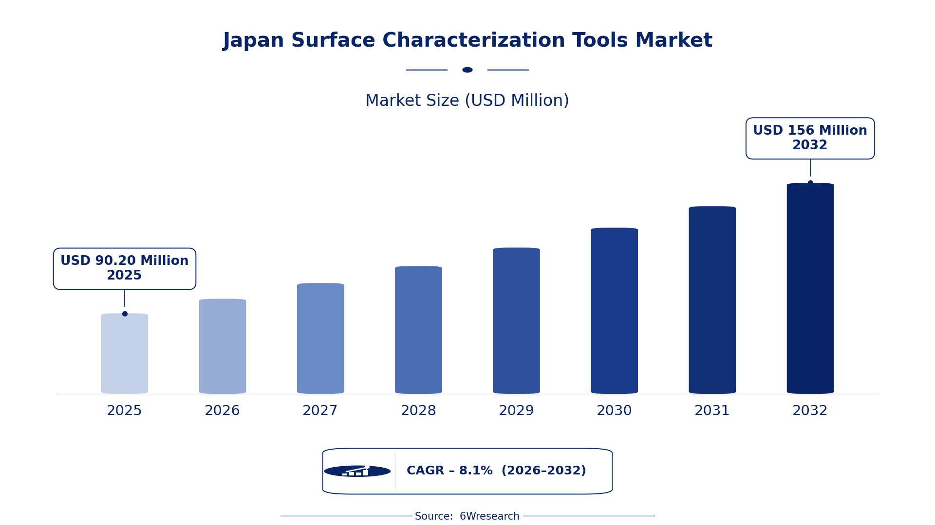
According to 6Wresearch internal database and industry insights, the Japan Surface Characterization Tools Market was valued at USD 90.20 Million in 2025 and is projected to reach USD 156 Million by 2032, growing at a CAGR of approximately 8.1% during 2026–2032.
Japan Surface Characterization Tools Market Highlights
| Report Metric | Details |
| Report Name | Japan Surface Characterization Tools Market (2026-2032) |
| Market Size 2025 | USD 90.20 Million |
| Market Size 2032 | USD 156 Million |
| Absolute Growth 2025–2032 | USD 65.80 Million |
| CAGR 2026–2032 | 8.1% |
| Peak Annual Growth | 9.0% in 2028 |
| Forecast Period | 2026–2032 |
| Historical Data | 2022–2025 |
| Base Year | 2025 |
| Leading Tool Type, 2025 | AFM (Atomic Force) (33% share) |
| Leading Analysis Method, 2025 | Topographical Mapping (43% share) |
| Leading Application Area, 2025 | Semiconductor Wafers (44% share) |
| Leading End User, 2025 | Research Labs (44% share) |
| Fastest-Growing Tool Type | XPS (X-ray Photoelectron) (11.3% CAGR) |
| Fastest-Growing Analysis Method | Chemical Composition (11.5% CAGR) |
| Fastest-Growing Application Area | Thin Films (9.8% CAGR) |
| Fastest-Growing End User | Nanotech Companies (10.7% CAGR) |
| Growing Sector | semiconductor manufacturing |
| Key End Users | research labs, electronics manufacturers, nanotech companies, surface engineering firms |
Japan Surface Characterization Tools Market Year-wise Growth Rate and Key Drivers (2022–2032)
This graph illustrates the annual growth rates of the market from 2022 to 2032, highlighting a steady upward trajectory and projected market expansion over the forecast period.
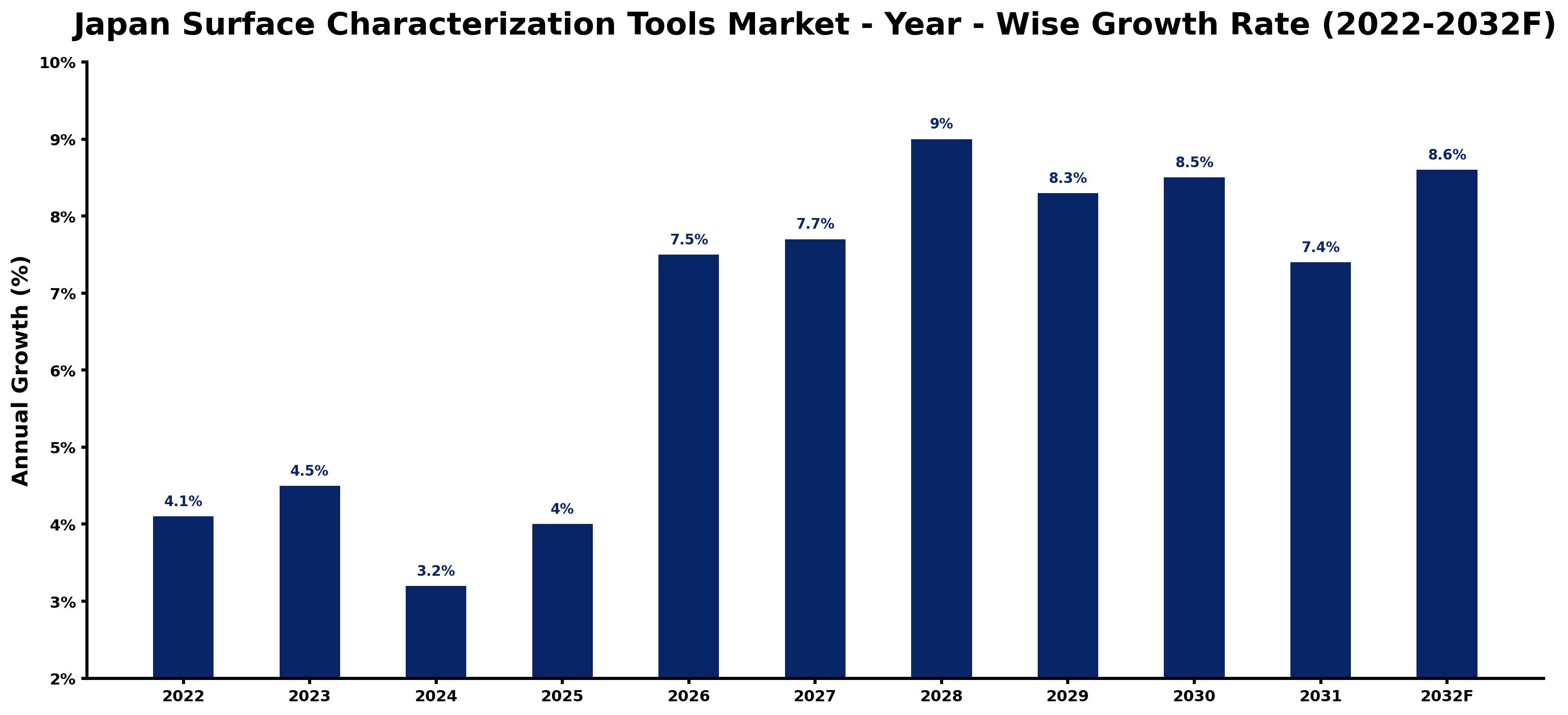
Each row of the following table gives one year's estimated growth and the event or demand shift that explains it.
| Year | Estimated Annual Growth (%) | Market Rationale |
| 2022 | 4.1 | The market showed steady growth due to ongoing demand from research labs. |
| 2023 | 4.5 | Growth accelerated as semiconductor projects expanded, increasing tool requirements. |
| 2024 | 3.2 | A slowdown occurred as some projects faced delays in funding and execution. |
| 2025 | 4.0 | Demand rose again as research labs initiated new surface characterization projects. |
| 2026 | 7.5 | Investment surged as the government allocated funds for semiconductor technology development. |
| 2027 | 7.7 | Continued investment in nanotechnology spurred further demand for characterization tools. |
| 2028 | 9.0 | Peak growth is expected to occur due to heightened activity in semiconductor manufacturing. |
| 2029 | 8.3 | Growth is projected to slow as market saturation begins to affect new tool purchases. |
| 2030 | 8.5 | Demand is anticipated to increase again as research labs expand their capabilities. |
| 2031 | 7.4 | A slowdown is expected as some sectors adjust to market conditions. |
| 2032 | 8.6 | Demand is projected to rise as new technologies are adopted in research. |
Note: Market size estimations and growth projections presented in this report are based on 6Wresearch's proprietary forecasting methodology, utilizing the latest available industry data, government publications, and primary research inputs.
Japan Surface Characterization Tools Market Synopsis
Surface characterization tools are essential instruments for analysing the surface properties of materials at micro and nano scales, primarily used in semiconductor manufacturing and research. The Japan Surface Characterization Tools Market is expanding, driven by a semiconductor market valued at approximately 4 trillion yen in 2022 and over 500 active research projects. Factors such as increased investment in semiconductor technology and the growing number of nanotech companies are propelling demand for these advanced instruments.
Market Dynamics Impact Analysis (2026–2032)
| Factor | Type | Impact | Primary Segment Affected |
| Increased investment in semiconductor technology development | Driver | High | AFM (Atomic Force) |
| Growing number of active research projects in surface analysis | Driver | High | XPS (X-ray Photoelectron) |
| Rising demand for advanced tools in nanotechnology | Opportunity | High | Nanotech Companies |
| Expansion of semiconductor manufacturing facilities | Opportunity | Medium | Semiconductor Wafers |
| High costs associated with advanced characterization tools | Restraint | High | SEM (Scanning Electron) |
| Limited availability of skilled technicians for tool operation | Restraint | Medium | Contact Angle Meters |
| Competition from alternative surface analysis technologies | Challenge | High | Chemical Composition |
| Fluctuations in government funding for research initiatives | Challenge | Medium | Research Labs |
Evaluation of Drivers in Japan Surface Characterization Tools Market (2026–2032)
The main growth drivers and the segments they affect most are set out below.
| Drivers | Primary Segment Affected | Why It Matters (Evidence) |
| Government investment in semiconductor technology | AFM (Atomic Force) | In 2023, the government allocated 10 billion yen for semiconductor technology development, increasing demand for advanced tools. |
| Expansion of research projects in surface characterization | XPS (X-ray Photoelectron) | Research labs in Japan have over 500 active projects, driving the need for XPS tools. |
| Growth in nanotechnology research funding | Nanotech Companies | Investment in nanotechnology research reached 50 billion yen in 2022, boosting demand for surface characterization tools. |
| Rising semiconductor manufacturing activities | Semiconductor Wafers | Japan's semiconductor market was valued at approximately 4 trillion yen in 2022, leading to increased purchases of characterization tools. |
| Focus on quality assurance in electronics manufacturing | Contact Angle Meters | ISO 9001 certification is commonly pursued by electronics manufacturers, increasing demand for quality control tools. |
Research labs have over 500 active projects, driving the need for X-ray Photoelectron tools. Investment in nanotechnology research hit 50 billion yen in 2022, increasing demand from nanotech companies. Japan's semiconductor market was valued at approximately 4 trillion yen in 2022, prompting more purchases of characterization instruments. Electronics manufacturers pursue ISO 9001 certification, increasing the need for quality assurance tools like contact angle meters.
Evaluation of Restraints in Japan Surface Characterization Tools Market
The following restraints limit how fast demand can grow.
| Market Restraint | Primary Segment Affected | Why It Matters (Evidence) |
| High costs of advanced characterization tools | SEM (Scanning Electron) | The installed base of SEM tools is approximately 1,500 units, indicating high costs can limit new purchases. |
| Shortage of skilled technicians for operation | Contact Angle Meters | Limited availability of skilled technicians affects the effective use of contact angle meters in research labs. |
| Competition from alternative surface analysis technologies | Chemical Composition | Emerging technologies may divert demand away from traditional characterization methods. |
| Fluctuations in government funding for research initiatives | Research Labs | Changes in funding can delay or reduce the number of projects requiring characterization tools. |
| Market saturation in certain segments | Nanotech Companies | An increasing number of nanotech companies may lead to competition that affects pricing and demand. |
Japan Surface Characterization Tools Market Challenges
A shortage of local suppliers for surface characterization tools in Japan creates supply chain disruptions, delaying projects for research institutions. Intense price competition among manufacturers squeezes profit margins, limiting funds for innovation and hampering producers' growth. A deficit of skilled technicians in advanced analysis techniques slows project turnarounds, negatively impacting productivity for electronics manufacturers. Adhering to the JIS Z 8801 standard increases operational costs, making it difficult for smaller firms to compete effectively in the market.
Trends in the Japan Surface Characterization Tools Market
Buyers and suppliers in the Japan Surface Characterization Tools Market are adjusting to the following trends.
- Shift towards Advanced Nanotechnology Research: Investment in nanotechnology research has surged, with over 300 nanotech companies in Japan driving demand for advanced characterization tools. This trend is expected to continue as the industry grows.
- Transition from Traditional to Modern Surface Analysis Techniques: Research institutions are moving towards modern surface analysis techniques, such as AFM and XPS, to improve accuracy and efficiency in their studies. This shift is reflected in the increasing adoption rates.
- Emergence of Sustainable Coating Technologies: Surface engineering firms are focusing on sustainable coating technologies, responding to environmental concerns. This trend is supported by the Japan Society of Applied Physics, which promotes research initiatives.
- Prioritisation of Quality Assurance in Electronics Manufacturing: Electronics manufacturers are increasingly prioritising quality assurance processes, resulting in higher demand for surface characterization tools. This trend aligns with the pursuit of ISO 9001 certification.
Investment Opportunities in the Japan Surface Characterization Tools Market
Investors looking at the Japan Surface Characterization Tools Market should consider the following areas.
- Research Labs seeking advanced characterization tools: Research labs require advanced surface characterization tools to support over 500 active projects. This presents a strong opportunity for suppliers to offer effective solutions.
- Rising demand for X-ray Photoelectron tools: The demand for X-ray Photoelectron tools is growing due to intensified research activities. Suppliers can enter the market by forming partnerships with research institutions.
- Entry into the semiconductor manufacturing sector: With Japan's semiconductor market valued at approximately 4 trillion yen, there is a pressing need for characterization tools. Collaborating with semiconductor manufacturers can provide a viable entry route.
- Investment in sustainable coating technologies: Surface engineering firms are prioritising sustainable technologies, creating opportunities for suppliers. The current trend towards sustainability makes this an ideal time for investment.
Government Initiatives in the Japan Surface Characterization Tools Market
The Economic Security Promotion Act, enacted in 2022, supports supply-chain resilience for critical products, including surface characterization tools. This measure ensures that producers and buyers can rely on a stable supply of essential materials, which is vital for market growth. The government allocated 10 billion yen in 2023 to support semiconductor technology development, benefiting both producers and buyers of characterization tools.
The National Institute of Advanced Industrial Science and Technology (AIST) oversees the implementation of the PRTR Law, which requires businesses to report chemical substance releases. This law impacts surface characterization tool producers, as they must comply with these regulations to ensure safe practices.
Future Insight of the Japan Surface Characterization Tools Market
Emerging technologies in surface analysis will notably alter demand for characterization tools, especially in aerospace materials research. The Japanese government's allocation of 10 billion yen for semiconductor technology development will stimulate innovation and open new avenues for suppliers. Strengthened collaborations between research institutions and industry will advance sustainable coating technologies. A growing focus on ISO 9001 certification will elevate quality standards, benefiting both buyers and suppliers in the market.
Market Segmentation Analysis
Japan Surface Characterization Tools Market report covers a detailed analysis of the following market segments:
By Tool Type – AFM (Atomic Force) Leads, XPS (X-ray Photoelectron) Expected to Grow Fastest
According to Saurav Kr Singh, Senior Research Analyst at 6Wresearch, AFM (Atomic Force) held 33% of the Japan Surface Characterization Tools Market by tool type in 2025. AFM holds the largest share because it is widely used in research labs for high-resolution imaging of surfaces, particularly in semiconductor applications. The technology's adoption rate of over 70% underscores its critical role in quality control processes within Japan's semiconductor market. XPS (X-ray Photoelectron) is set to record the highest CAGR in this split, 11.3% over 2026–2032. The growth of XPS is propelled by its essential function in chemical composition analysis, especially for the semiconductor sector valued at approximately 4 trillion yen in 2022. As research demands intensify, the relevance of this tool in advanced material studies will continue to expand. Suppliers should prioritise increasing the availability of XPS tools to address the growing demand in research institutions.
By Analysis Method – Topographical Mapping Leads, Chemical Composition Expected to Grow Fastest
The largest analysis method category in 2025 was Topographical Mapping, at 43% of revenue. Topographical Mapping holds the largest share because it is essential for understanding surface roughness and features, particularly in semiconductor manufacturing. Its critical role in quality assurance makes it a preferred choice among research labs across Japan. Chemical Composition is projected to grow fastest, at a CAGR of 11.5% during 2026–2032. The growth of Chemical Composition analysis is propelled by its importance in material characterization, especially within the semiconductor sector that is experiencing significant investment. This method's relevance in ongoing research projects will likely encourage further adoption. Suppliers should focus on enhancing their offerings in topographical mapping to meet the demands of research labs.
By Application Area – Semiconductor Wafers Lead, Thin Films Expected to Grow Fastest
In 2025, Semiconductor Wafers led the application area split with a 44% share. Semiconductor Wafers dominate the market as they are critical in semiconductor manufacturing processes, which are a cornerstone of Japan's electronics industry. The substantial installed base of tools for this application reflects its importance in quality control. Over 2026–2032, Thin Films are expected to post the fastest growth, at a CAGR of 9.8%. Thin Films are experiencing rapid growth due to their extensive use in coatings and electronics applications, driven by the increasing number of nanotech companies in Japan. This segment's expansion is supported by ongoing research and development initiatives. Suppliers should prioritise innovations in tools for thin film analysis to capture the growing market opportunities.
By End User – Research Labs Lead, Nanotech Companies Expected to Grow Fastest
Research Labs accounted for 44% of the market by end user in 2025. Research Labs represent the largest user group as they are the primary consumers for experimental and analytical purposes, significantly impacting the demand for surface characterization tools. With over 500 active projects, these labs play a crucial role in advancing surface engineering research in Japan. The quickest growth will come from Nanotech Companies, forecast to expand at a CAGR of 10.7% between 2026 and 2032. Nanotech Companies are the fastest-growing segment due to their focus on developing advanced materials and applications that require sophisticated surface characterization tools. The increasing investment in nanotechnology research is a significant factor driving this growth. Suppliers need to tailor their products to meet the specific needs of nanotech companies to leverage this expanding market.
Key Attractiveness of the Report
- 10 Years of Market Numbers
- Historical Data Starting from 2022 to 2025
- Base Year 2025
- Forecast Data until 2032
- Key Performance Indicators Impacting the Market
- Major Upcoming Developments and Projects
Key Highlights of the Report:
- Japan Surface Characterization Tools Market Outlook
- Market Size of Japan Surface Characterization Tools Market, 2025
- Forecast of Japan Surface Characterization Tools Market, 2032
- Historical Data and Forecast of Japan Surface Characterization Tools Revenues & Volume for the Period 2022-2032F
- Japan Surface Characterization Tools Market Trend Evolution
- Japan Surface Characterization Tools Market Drivers and Challenges
- Japan Surface Characterization Tools Price Trends
- Japan Surface Characterization Tools Porter's Five Forces
- Japan Surface Characterization Tools Industry Life Cycle
- Historical Data and Forecast of Japan Surface Characterization Tools Market Revenues & Volume By Tool Type for the Period 2022-2032F
- Historical Data and Forecast of Japan Surface Characterization Tools Market Revenues & Volume By AFM (Atomic Force) for the Period 2022-2032F
- Historical Data and Forecast of Japan Surface Characterization Tools Market Revenues & Volume By XPS (X-ray Photoelectron) for the Period 2022-2032F
- Historical Data and Forecast of Japan Surface Characterization Tools Market Revenues & Volume By SEM (Scanning Electron) for the Period 2022-2032F
- Historical Data and Forecast of Japan Surface Characterization Tools Market Revenues & Volume By Contact Angle Meters for the Period 2022-2032F
- Historical Data and Forecast of Japan Surface Characterization Tools Market Revenues & Volume By Analysis Method for the Period 2022-2032F
- Historical Data and Forecast of Japan Surface Characterization Tools Market Revenues & Volume By Topographical Mapping for the Period 2022-2032F
- Historical Data and Forecast of Japan Surface Characterization Tools Market Revenues & Volume By Chemical Composition for the Period 2022-2032F
- Historical Data and Forecast of Japan Surface Characterization Tools Market Revenues & Volume By Morphology Analysis for the Period 2022-2032F
- Historical Data and Forecast of Japan Surface Characterization Tools Market Revenues & Volume By Wettability for the Period 2022-2032F
- Historical Data and Forecast of Japan Surface Characterization Tools Market Revenues & Volume By Application Area for the Period 2022-2032F
- Historical Data and Forecast of Japan Surface Characterization Tools Market Revenues & Volume By Semiconductor Wafers for the Period 2022-2032F
- Historical Data and Forecast of Japan Surface Characterization Tools Market Revenues & Volume By Thin Films for the Period 2022-2032F
- Historical Data and Forecast of Japan Surface Characterization Tools Market Revenues & Volume By Circuit Boards for the Period 2022-2032F
- Historical Data and Forecast of Japan Surface Characterization Tools Market Revenues & Volume By Coating Research for the Period 2022-2032F
- Historical Data and Forecast of Japan Surface Characterization Tools Market Revenues & Volume By End User for the Period 2022-2032F
- Historical Data and Forecast of Japan Surface Characterization Tools Market Revenues & Volume By Research Labs for the Period 2022-2032F
- Historical Data and Forecast of Japan Surface Characterization Tools Market Revenues & Volume By Nanotech Companies for the Period 2022-2032F
- Historical Data and Forecast of Japan Surface Characterization Tools Market Revenues & Volume By Electronics Manufacturers for the Period 2022-2032F
- Historical Data and Forecast of Japan Surface Characterization Tools Market Revenues & Volume By Surface Engineering Firms for the Period 2022-2032F
- Japan Surface Characterization Tools Import Export Trade Statistics
- Market Opportunity Assessment By Tool Type
- Market Opportunity Assessment By Analysis Method
- Market Opportunity Assessment By Application Area
- Market Opportunity Assessment By End User
- Japan Surface Characterization Tools Top Companies Market Share
- Japan Surface Characterization Tools Competitive Benchmarking By Technical and Operational Parameters
- Japan Surface Characterization Tools Company Profiles
- Japan Surface Characterization Tools Key Strategic Recommendations
Market Covered
The following segment groups are covered in the report.
By Tool Type
- AFM (Atomic Force)
- XPS (X-ray Photoelectron)
- SEM (Scanning Electron)
- Contact Angle Meters
By Analysis Method
- Topographical Mapping
- Chemical Composition
- Morphology Analysis
- Wettability
By Application Area
- Semiconductor Wafers
- Thin Films
- Circuit Boards
- Coating Research
By End User
- Research Labs
- Nanotech Companies
- Electronics Manufacturers
- Surface Engineering Firms