Japan Thin Film Deposition Market Size & Growth Rate
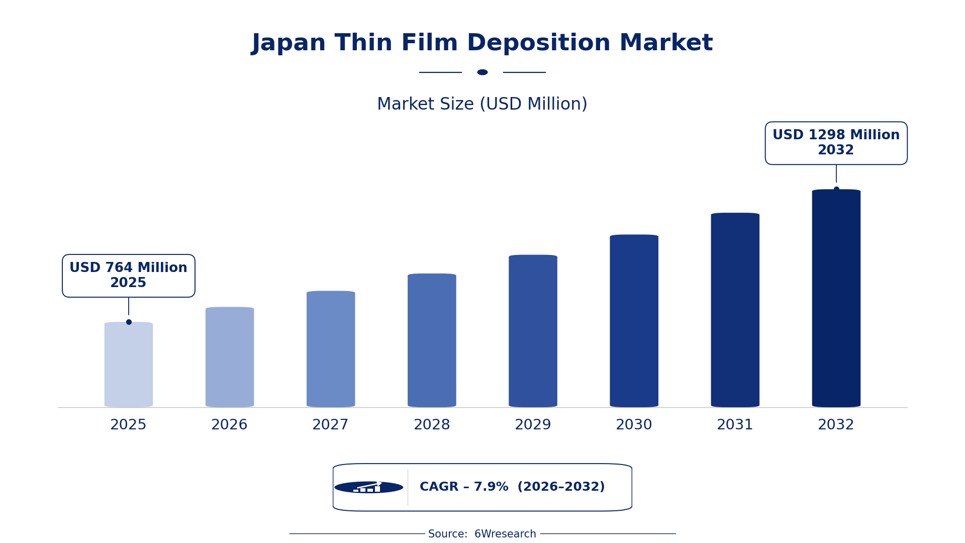
According to 6Wresearch internal database and industry insights, the Japan Thin Film Deposition Market was valued at USD 764 Million in 2025 and is projected to reach USD 1,298 Million by 2032, growing at a CAGR of approximately 7.9% during 2026–2032.
Japan Thin Film Deposition Market Highlights
| Report Metric | Details |
| Report Name | Japan Thin Film Deposition Market (2026-2032) |
| Market Size 2025 | USD 764 Million |
| Market Size 2032 | USD 1,298 Million |
| Absolute Growth 2025–2032 | USD 534 Million |
| CAGR 2026–2032 | 7.9% |
| Peak Annual Growth | 8.2% in 2028 |
| Forecast Period | 2026–2032 |
| Historical Data | 2022–2025 |
| Base Year | 2025 |
| Leading Deposition Type, 2025 | Chemical Vapor Deposition (CVD) (50% share) |
| Leading Material Type, 2025 | Metals (50% share) |
| Leading Technology Used, 2025 | Sputtering (40% share) |
| Leading End User, 2025 | Semiconductor Foundries (49% share) |
| Fastest-Growing Deposition Type | Atomic Layer Deposition (ALD) (10.7% CAGR) |
| Fastest-Growing Material Type | Nanolayers (11.2% CAGR) |
| Fastest-Growing Technology Used | Atomic Precision (11.7% CAGR) |
| Fastest-Growing End User | R&D Labs (10.3% CAGR) |
| Growing Sector | Semiconductor manufacturing |
| Key End Users | Semiconductor Foundries, Display Panel Producers, Solar Cell Firms, R&D Labs |
Japan Thin Film Deposition Market Year-wise Growth Rate and Key Drivers (2022–2032)
This graph illustrates the annual growth rates of the market from 2022 to 2032, highlighting a steady upward trajectory and projected market expansion over the forecast period.
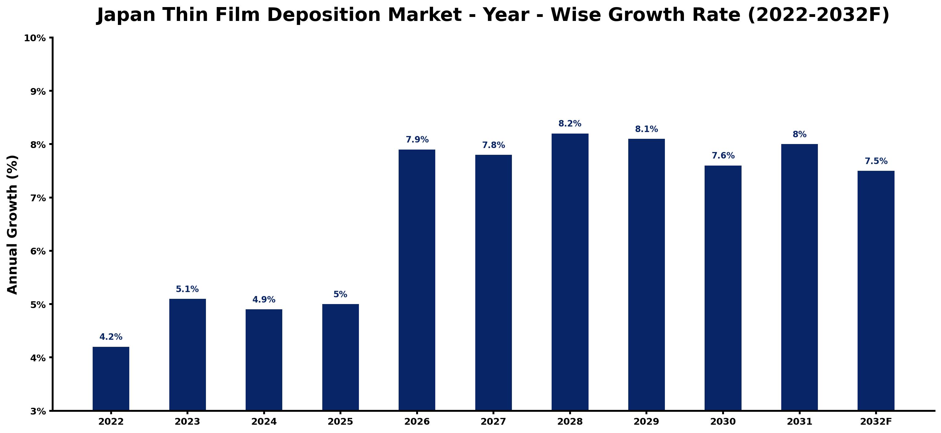
For each year, the table pairs the estimated growth rate with the leading influence on demand, showing how the drivers changed across the period.
| Year | Estimated Annual Growth (%) | Market Rationale |
| 2022 | 4.2 | The market experienced steady growth due to ongoing demand from semiconductor foundries. |
| 2023 | 5.1 | Growth accelerated as production increased in response to global semiconductor demand. |
| 2024 | 4.9 | Growth slowed slightly due to adjustments following the previous year's peak. |
| 2025 | 5.0 | Demand rose again as investments in semiconductor innovation gained traction. |
| 2026 | 7.9 | The market growth rate is expected to increase due to rising investments in semiconductor R&D. |
| 2027 | 7.8 | A slight slowdown is projected as the market adjusts to previous growth levels. |
| 2028 | 8.2 | Demand is expected to surge as advanced deposition technologies gain wider adoption. |
| 2029 | 8.1 | Growth is projected to decelerate slightly due to market saturation effects. |
| 2030 | 7.6 | The market is expected to continue growing, albeit at a slower pace due to increased competition. |
| 2031 | 8.0 | Demand will increase again as new technologies emerge in the semiconductor sector. |
| 2032 | 7.5 | Growth is projected to slow as the market stabilises after rapid advancements. |
Note: Market size estimations and growth projections presented in this report are based on 6Wresearch's proprietary forecasting methodology, utilizing the latest available industry data, government publications, and primary research inputs.
Japan Thin Film Deposition Market Synopsis
Thin film deposition is a technology for applying thin layers of material in sectors such as semiconductor manufacturing, display technologies, and solar cells. In Japan, over 50 semiconductor foundries in the Kanto region drive demand, supported by investments in R&D, which reached 200 billion yen in 2023. The Ministry of Economy, Trade and Industry has also launched a programme to support semiconductor innovation. These elements suggest strong growth potential for the Japan Thin Film Deposition Market.
Market Dynamics Impact Analysis (2026–2032)
| Factor | Type | Impact | Primary Segment Affected |
| Increasing semiconductor production capacity | Driver | High | Physical Vapor Deposition (PVD) |
| Rising demand for high-quality thin films in electronics | Driver | High | Chemical Vapor Deposition (CVD) |
| Growing investment in nanotechnology applications | Opportunity | Medium | Nanolayers |
| Expansion of solar energy initiatives | Opportunity | Medium | Solar Cell Firms |
| High competition among deposition technology providers | Restraint | High | Atomic Layer Deposition (ALD) |
| Challenges in meeting stringent quality standards | Restraint | Medium | Metals |
| Supply chain disruptions affecting material availability | Challenge | High | Sputtering |
| Technological advancements requiring constant adaptation | Challenge | Medium | Plasma-Enhanced |
Evaluation of Drivers in Japan Thin Film Deposition Market (2026–2032)
The factors lifting demand, and the evidence behind each, are summarised below.
| Drivers | Primary Segment Affected | Why It Matters (Evidence) |
| Rising semiconductor manufacturing | Physical Vapor Deposition (PVD) | Japan's semiconductor foundries, over 50 in the Kanto region, drive demand for PVD processes. |
| Demand for high-quality films in electronics | Chemical Vapor Deposition (CVD) | Numerous display panel producers in the Tokyo metropolitan area require CVD for quality films. |
| Investment in nanotechnology | Nanolayers | Japan ranks among the top countries in thin film technology patents, boosting applications for nanolayers. |
| Solar energy production growth | Solar Cell Firms | In 2023, Japan's solar cell production reached 1.5 GW, increasing demand for thin film technologies. |
| Technological advancements in deposition | Atomic Layer Deposition (ALD) | Research hubs like the University of Tokyo focus on ALD techniques for precision in semiconductor devices. |
Buyers are adding capacity as semiconductor manufacturing expands, with over 50 foundries located in the Kanto region. In 2023, Japan's solar cell production reached 1.5 GW, driving demand for thin film technologies. Investment in semiconductor R&D reached 200 billion yen, supporting production capabilities. The Tokyo metropolitan area hosts numerous display panel producers, increasing the need for high-quality thin films. Research on atomic layer deposition techniques at institutions like the University of Tokyo advances precision manufacturing.
Evaluation of Restraints in Japan Thin Film Deposition Market
The following restraints limit how fast demand can grow.
| Market Restraint | Primary Segment Affected | Why It Matters (Evidence) |
| Intense competition among technology providers | Atomic Layer Deposition (ALD) | Numerous providers create price pressures, impacting profitability for suppliers. |
| Difficulty in meeting quality standards | Metals | Adhering to ISO 9001 standards necessitates rigorous quality control that can delay production. |
| Supply chain disruptions | Sputtering | Global supply chain issues affect the availability of essential materials for sputtering processes. |
| Technological adaptation challenges | Plasma-Enhanced | Rapid technological advancements require constant updates, straining resources for manufacturers. |
| High operational costs for R&D | Nanolayers | Investment in advanced nanotechnology applications can be prohibitively expensive for smaller firms. |
Japan Thin Film Deposition Market Challenges
Japan's thin film deposition market faces a technology gap, as outdated methods can delay production timelines for semiconductor foundries by up to six months. Local producers encounter fierce competition from nations with lower production costs, forcing them to reduce prices and risking profit margins, which limits their R&D investments. A shortage of skilled technicians in advanced deposition techniques leads to production inefficiencies, potentially causing output losses of 15% for display panel manufacturers. Stringent environmental regulations increase compliance costs, burdening buyers with additional expenses of around 5% on their procurement budgets.
Trends in the Japan Thin Film Deposition Market
Several trends are reshaping the Japan Thin Film Deposition Market; the most important are set out below.
- Shift in Semiconductor Manufacturing: Japan's semiconductor foundries are increasingly adopting atomic layer deposition techniques, improving precision in production. In 2023, over 50 foundries were operational, indicating a strong shift towards advanced technologies.
- Focus on Renewable Energy: Solar cell firms are prioritising thin film technologies, with production reaching 1.5 GW in 2023. This trend highlights the growing demand for efficient solar energy solutions in Japan.
- Increased Investment in R&D: Investment in semiconductor R&D reached 200 billion yen in 2023, reflecting a strong commitment to innovation. This trend supports the development of advanced deposition technologies across industries.
- Adoption of JIS Standards: Japanese manufacturers are increasingly adhering to JIS standards for thin film processes, ensuring high-quality production. This shift is important for maintaining competitiveness in global markets.
Investment Opportunities in the Japan Thin Film Deposition Market
The openings below show where demand in the Japan Thin Film Deposition Market is visible and how suppliers can enter.
- Semiconductor Foundries Seeking Innovation: Semiconductor foundries are investing in advanced deposition technologies, with R&D investments reaching 200 billion yen in 2023. Collaborating with local research institutions can facilitate innovation.
- Rising Demand for High-Quality Thin Films: The demand for high-quality thin films is increasing, particularly in display technologies. Suppliers can target the Tokyo metropolitan area, where numerous display panel producers operate.
- Investment in Solar Technology: Solar cell firms are expanding their production capabilities, with Japan's installed base of solar panels surpassing 75 GW in 2023. Entering partnerships with these firms can yield opportunities.
- Focus on Nanotechnology Applications: The growing interest in nanotechnology presents opportunities for suppliers of nanolayers. Engaging with R&D labs in Japan can lead to innovative applications and market entry.
Government Initiatives in the Japan Thin Film Deposition Market
The Plastic Resource Circulation Act, enacted in 2021, impacts producers by mandating the reduction, reuse, and recycling of plastics, which affects the materials used in thin film deposition. Compliance requires manufacturers to invest in sustainable practices and technologies, influencing production costs. Additionally, the Act on the Rational Use of Energy obliges large energy users to improve energy efficiency, prompting thin film producers to adopt energy-efficient technologies to meet regulatory standards, thus enhancing their operational efficiency.
The Ministry of Economy, Trade and Industry oversees the Advanced Semiconductor Technology Program, which funds projects aimed at enhancing domestic semiconductor production capabilities. In 2023, this initiative allocated significant resources to support innovation in thin film deposition techniques, benefiting semiconductor foundries and R&D labs. By facilitating access to advanced technologies, this programme enables buyers to enhance their production processes and maintain competitiveness in the global market.
Future Insight of the Japan Thin Film Deposition Market
The emergence of cutting-edge manufacturing technologies will reshape demand for thin film deposition in electronics, driving improvements in product performance. By 2032, the establishment of new research facilities will support innovation in semiconductor applications, benefiting local producers. Japan's focus on renewable energy will further boost the solar sector, with solar panel installations expected to exceed 100 GW, creating opportunities for thin film technologies. Continued government support through programmes will strengthen domestic production capabilities, ensuring competitiveness in the global market.
Market Segmentation Analysis
Japan Thin Film Deposition Market report covers a detailed analysis of the following market segments:
By Deposition Type – Chemical Vapor Deposition (CVD) Leads, Atomic Layer Deposition (ALD) Expected to Grow Fastest
According to Saurav Kr Singh, Senior Research Analyst at 6Wresearch, Chemical Vapor Deposition (CVD) held 50% of the Japan Thin Film Deposition Market by deposition type in 2025. Chemical Vapor Deposition holds the largest share as it is essential for producing high-quality thin films used in semiconductor manufacturing. This technique is prevalent in Japan's semiconductor foundries, particularly in the Kanto region, which is a key area for technological advancement. Over 2026–2032, Atomic Layer Deposition (ALD) is expected to post the fastest growth, at a CAGR of 10.7%. Atomic Layer Deposition is witnessing rapid growth due to its critical role in achieving atomic-scale precision for semiconductor devices. The substantial investment in semiconductor R&D, which reached 200 billion yen in 2023, is expected to further accelerate this growth. Suppliers should prioritise advancements in Atomic Layer Deposition to leverage its expanding market opportunities.
By Material Type – Metals Lead, Nanolayers Expected to Grow Fastest
Metals took 50% of material type revenue in 2025, more than any other category. Metals lead the market because they are fundamental for the production of electronic components and circuits vital for various technologies. Their extensive application in Japan's semiconductor and electronics industries reinforces their dominant position. The quickest growth will come from Nanolayers, forecast to expand at a CAGR of 11.2% between 2026 and 2032. Nanolayers are the fastest-growing segment as they are crucial for advanced electronic and optical devices, driven by the increasing demand for miniaturisation and improved performance. This growth is reflected in ongoing research efforts in nanotechnology. Buyers should explore investments in nanolayer technologies to maintain a competitive edge in the electronics sector.
By Technology Used – Sputtering Leads, Atomic Precision Expected to Grow Fastest
With 40% of technology used revenue in 2025, Sputtering was the largest category. Sputtering is the leading technology as it is a common technique employed in semiconductor manufacturing processes across Japan's extensive foundry network. Its established reliability and effectiveness make it a preferred choice among manufacturers. Atomic Precision is projected to grow fastest, at a CAGR of 11.7% during 2026–2032. Atomic Precision is growing rapidly because it is vital for next-generation semiconductor technologies that require higher performance and efficiency. The emphasis on advanced techniques in R&D labs is propelling this segment forward. Suppliers must innovate in Atomic Precision technologies to meet the rising demand from semiconductor manufacturers.
By End User – Semiconductor Foundries Lead, R&D Labs Expected to Grow Fastest
Semiconductor Foundries accounted for 49% of the market by end user in 2025. Semiconductor Foundries represent the largest end user group, as they are the major consumers of thin film deposition technologies necessary for chip production. The concentration of over 50 foundries in Japan highlights the critical role they play in the market. R&D Labs are set to record the highest CAGR in this split, 10.3% over 2026–2032. R&D Labs are the fastest-growing end user segment, driven by their focus on researching advanced deposition techniques to support emerging technologies. The investment in semiconductor innovation programmes is fuelling this growth. Suppliers should engage with R&D Labs to align their products with future technological advancements.
Key Attractiveness of the Report
- 10 Years of Market Numbers
- Historical Data Starting from 2022 to 2025
- Base Year 2025
- Forecast Data until 2032
- Key Performance Indicators Impacting the Market
- Major Upcoming Developments and Projects
Key Highlights of the Report:
- Japan Thin Film Deposition Market Outlook
- Market Size of Japan Thin Film Deposition Market, 2025
- Forecast of Japan Thin Film Deposition Market, 2032
- Historical Data and Forecast of Japan Thin Film Deposition Revenues & Volume for the Period 2022-2032F
- Japan Thin Film Deposition Market Trend Evolution
- Japan Thin Film Deposition Market Drivers and Challenges
- Japan Thin Film Deposition Price Trends
- Japan Thin Film Deposition Porter's Five Forces
- Japan Thin Film Deposition Industry Life Cycle
- Historical Data and Forecast of Japan Thin Film Deposition Market Revenues & Volume By Deposition Type for the Period 2022-2032F
- Historical Data and Forecast of Japan Thin Film Deposition Market Revenues & Volume By Physical Vapor Deposition (PVD) for the Period 2022-2032F
- Historical Data and Forecast of Japan Thin Film Deposition Market Revenues & Volume By Chemical Vapor Deposition (CVD) for the Period 2022-2032F
- Historical Data and Forecast of Japan Thin Film Deposition Market Revenues & Volume By Atomic Layer Deposition (ALD) for the Period 2022-2032F
- Historical Data and Forecast of Japan Thin Film Deposition Market Revenues & Volume By Electrochemical Deposition for the Period 2022-2032F
- Historical Data and Forecast of Japan Thin Film Deposition Market Revenues & Volume By Material Type for the Period 2022-2032F
- Historical Data and Forecast of Japan Thin Film Deposition Market Revenues & Volume By Metals for the Period 2022-2032F
- Historical Data and Forecast of Japan Thin Film Deposition Market Revenues & Volume By Ceramics for the Period 2022-2032F
- Historical Data and Forecast of Japan Thin Film Deposition Market Revenues & Volume By Nanolayers for the Period 2022-2032F
- Historical Data and Forecast of Japan Thin Film Deposition Market Revenues & Volume By Conductive Inks for the Period 2022-2032F
- Historical Data and Forecast of Japan Thin Film Deposition Market Revenues & Volume By Technology Used for the Period 2022-2032F
- Historical Data and Forecast of Japan Thin Film Deposition Market Revenues & Volume By Sputtering for the Period 2022-2032F
- Historical Data and Forecast of Japan Thin Film Deposition Market Revenues & Volume By Plasma-Enhanced for the Period 2022-2032F
- Historical Data and Forecast of Japan Thin Film Deposition Market Revenues & Volume By Atomic Precision for the Period 2022-2032F
- Historical Data and Forecast of Japan Thin Film Deposition Market Revenues & Volume By Electrodeposition for the Period 2022-2032F
- Historical Data and Forecast of Japan Thin Film Deposition Market Revenues & Volume By End User for the Period 2022-2032F
- Historical Data and Forecast of Japan Thin Film Deposition Market Revenues & Volume By Semiconductor Foundries for the Period 2022-2032F
- Historical Data and Forecast of Japan Thin Film Deposition Market Revenues & Volume By Display Panel Producers for the Period 2022-2032F
- Historical Data and Forecast of Japan Thin Film Deposition Market Revenues & Volume By Solar Cell Firms for the Period 2022-2032F
- Historical Data and Forecast of Japan Thin Film Deposition Market Revenues & Volume By R&D Labs for the Period 2022-2032F
- Japan Thin Film Deposition Import Export Trade Statistics
- Market Opportunity Assessment By Deposition Type
- Market Opportunity Assessment By Material Type
- Market Opportunity Assessment By Technology Used
- Market Opportunity Assessment By End User
- Japan Thin Film Deposition Top Companies Market Share
- Japan Thin Film Deposition Competitive Benchmarking By Technical and Operational Parameters
- Japan Thin Film Deposition Company Profiles
- Japan Thin Film Deposition Key Strategic Recommendations
Market Covered
The study includes the following segmentation.
By Deposition Type
- Physical Vapor Deposition (PVD)
- Chemical Vapor Deposition (CVD)
- Atomic Layer Deposition (ALD)
- Electrochemical Deposition
By Material Type
- Metals
- Ceramics
- Nanolayers
- Conductive Inks
By Technology Used
- Sputtering
- Plasma-Enhanced
- Atomic Precision
- Electrodeposition
By End User
- Semiconductor Foundries
- Display Panel Producers
- Solar Cell Firms
- R&D Labs