Japan Wafer-Level Testing Market Size & Growth Rate
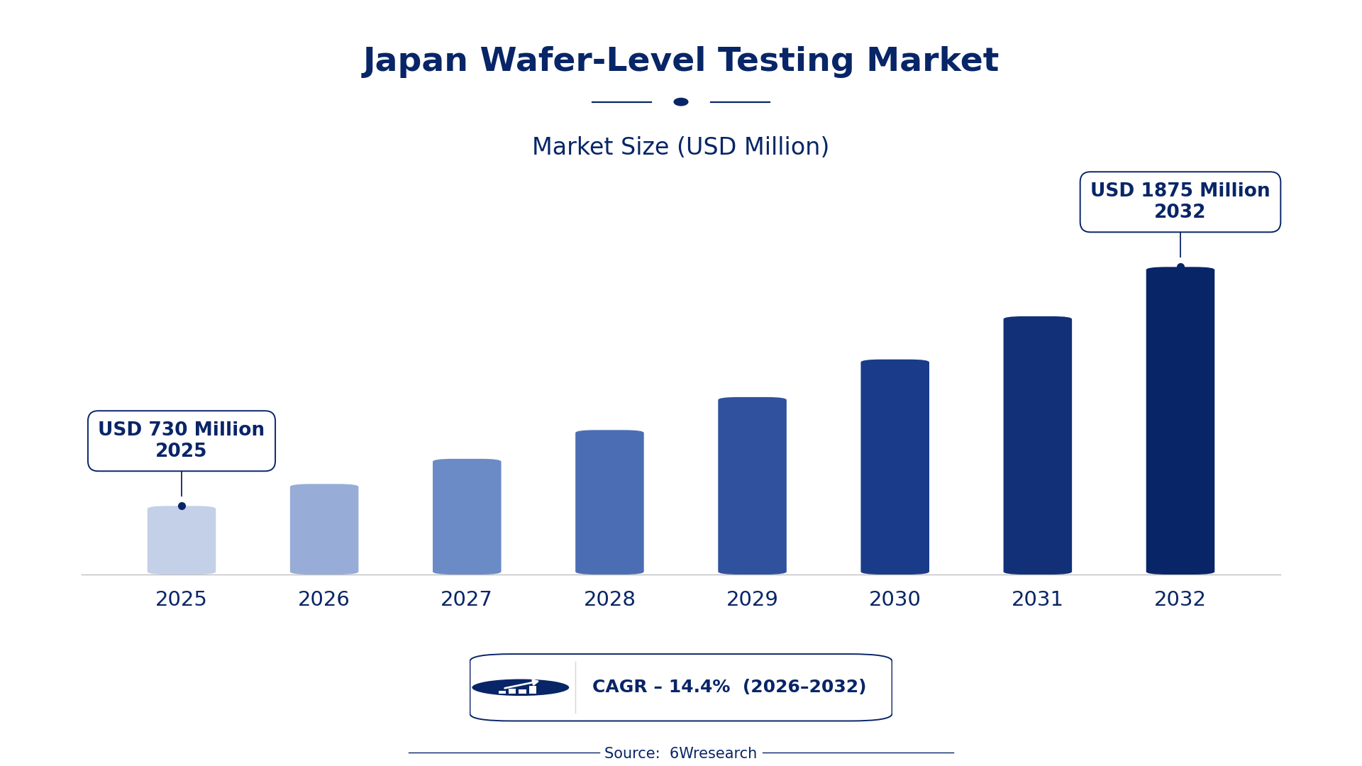
According to 6Wresearch internal database and industry insights, the Japan Wafer-Level Testing Market was valued at USD 730 Million in 2025 and is projected to reach USD 1,875 Million by 2032, growing at a CAGR of approximately 14.4% during 2026–2032.
Japan Wafer-Level Testing Market Highlights
| Report Metric | Details |
| Report Name | Japan Wafer-Level Testing Market (2026-2032) |
| Market Size 2025 | USD 730 Million |
| Market Size 2032 | USD 1,875 Million |
| Absolute Growth 2025–2032 | USD 1,145 Million |
| CAGR 2026–2032 | 14.4% |
| Peak Annual Growth | 15.7% in 2028 |
| Forecast Period | 2026–2032 |
| Historical Data | 2022–2025 |
| Base Year | 2025 |
| Leading Test Type, 2025 | Electrical Testing (40% share) |
| Leading Probe Card Type, 2025 | MEMS Probe (45% share) |
| Leading Equipment Format, 2025 | Automated Tester (48% share) |
| Leading Deployment Area, 2025 | Front-End Line (33% share) |
| Fastest-Growing Test Type | Optical Inspection (19.9% CAGR) |
| Fastest-Growing Probe Card Type | Optical Probes (19.6% CAGR) |
| Fastest-Growing Equipment Format | Inline Tester (20.0% CAGR) |
| Fastest-Growing Deployment Area | Wafer Fab Plants (16.7% CAGR) |
| Growing Sector | semiconductor manufacturing |
| Key End Users | semiconductor manufacturers, electronics producers, R&D laboratories |
Japan Wafer-Level Testing Market Year-wise Growth Rate and Key Drivers (2022–2032)
This graph illustrates the annual growth rates of the market from 2022 to 2032, highlighting a steady upward trajectory and projected market expansion over the forecast period.
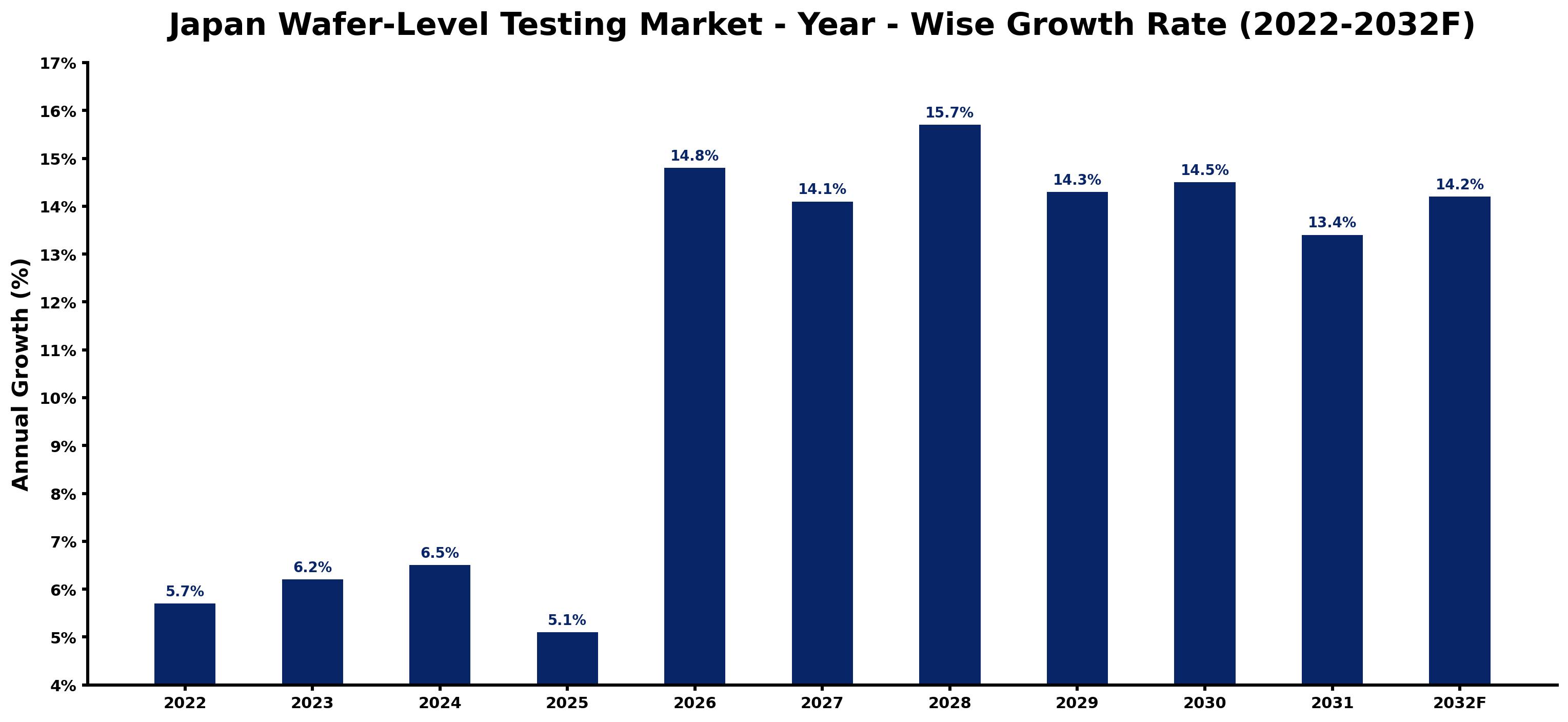
Below, each year's estimated growth is shown next to the factor that most influenced it.
| Year | Estimated Annual Growth (%) | Market Rationale |
| 2022 | 5.7 | The market showed solid growth with increasing investments in semiconductor technologies. |
| 2023 | 6.2 | Demand accelerated due to heightened focus on domestic semiconductor production. |
| 2024 | 6.5 | Growth continued as manufacturers sought to improve testing capabilities. |
| 2025 | 5.1 | A slight slowdown occurred as market adjustments took place after rapid expansion. |
| 2026 | 14.8 | Investment surged as companies aim to innovate and improve efficiency. |
| 2027 | 14.1 | Growth is expected to slow slightly as the market stabilises after previous peaks. |
| 2028 | 15.7 | The market is projected to peak due to technological advancements and demand. |
| 2029 | 14.3 | Growth is expected to decelerate as the market begins to normalise after peak performance. |
| 2030 | 14.5 | A rebound in demand is anticipated as new technologies are adopted widely. |
| 2031 | 13.4 | Growth is projected to slow again as the market approaches saturation levels. |
| 2032 | 14.2 | Demand is expected to rise again as new applications emerge. |
Note: Market size estimations and growth projections presented in this report are based on 6Wresearch's proprietary forecasting methodology, utilizing the latest available industry data, government publications, and primary research inputs.
Japan Wafer-Level Testing Market Synopsis
Wafer-Level Testing evaluates integrated circuits at the wafer level, ensuring quality control during manufacturing. The Japan Wafer-Level Testing Market is expanding, driven by domestic demand from semiconductor manufacturers and ongoing investments in R&D, with the industry valued at approximately 4 trillion yen. The recent programme launched by the Ministry of Economy, Trade and Industry to support semiconductor innovation is stimulating growth, leading to increased purchases of advanced testing equipment and improving production capabilities.
Market Dynamics Impact Analysis (2026–2032)
| Factor | Type | Impact | Primary Segment Affected |
| Rising investments in semiconductor R&D | Driver | High | Electrical Testing |
| Increased demand for high-quality semiconductors | Driver | High | Functional Testing |
| Growing need for advanced testing solutions | Opportunity | High | Optical Inspection |
| Expansion of wafer fab plants in key regions | Opportunity | Medium | Wafer Fab Plants |
| High costs of advanced testing equipment | Restraint | High | Automated Tester |
| Limited availability of skilled engineers | Restraint | Medium | MEMS Probe |
| Compliance with stringent industry standards | Challenge | High | Optical Inspection |
| Capacity constraints in production lines | Challenge | Medium | Front-End Line |
Evaluation of Drivers in Japan Wafer-Level Testing Market (2026–2032)
The main growth drivers and the segments they affect most are set out below.
| Drivers | Primary Segment Affected | Why It Matters (Evidence) |
| Increased funding for semiconductor R&D | Electrical Testing | Japan invests around 300 billion yen annually in semiconductor R&D, boosting demand for testing solutions. |
| Growing semiconductor exports | Functional Testing | Exports reached 1.5 trillion yen in 2022, driving the need for reliable testing methods. |
| Technological advancements in testing equipment | Optical Inspection | Innovations in testing methodologies improve the efficiency and accuracy of inspections, enhancing productivity. |
| Expansion of wafer fab plants | Wafer Fab Plants | With over 100 operational plants, the demand for testing services is expected to increase significantly. |
| Increasing production of microelectronic devices | MEMS Probe | Over 1 billion chips are produced annually, necessitating effective testing solutions to ensure quality. |
Purchasing is picking up as investments in semiconductor R&D reach approximately 300 billion yen annually, stimulating demand for advanced testing solutions. The growth in semiconductor exports, which reached 1.5 trillion yen in 2022, further drives the need for reliable testing methods. The expansion of wafer fab plants, with over 100 operational facilities, increases the demand for testing services. The production of over 1 billion microelectronic devices annually necessitates effective testing solutions, creating further opportunities for growth in the market.
Evaluation of Restraints in Japan Wafer-Level Testing Market
The key brakes on demand, and where they bite hardest, are shown below.
| Market Restraint | Primary Segment Affected | Why It Matters (Evidence) |
| High costs associated with advanced testing equipment | Automated Tester | The price of advanced testing equipment can exceed 100 million yen, limiting procurement. |
| Shortage of skilled semiconductor engineers | MEMS Probe | With around 50,000 engineers in Japan, the talent pool is insufficient to meet industry demands. |
| Compliance with stringent industry standards | Optical Inspection | Adhering to the JIS Q 7001 standard requires investment in training and certification, impacting budgets. |
| Capacity constraints in production lines | Front-End Line | Production lines often run at full capacity, limiting the ability to scale testing operations effectively. |
| Dependency on domestic semiconductor market | Functional Testing | Fluctuations in the domestic market can directly impact testing demand and revenue generation. |
Japan Wafer-Level Testing Market Challenges
Producers face high operational costs due to Japan's semiconductor industry being valued at approximately 4 trillion yen, limiting their investment in advanced testing technologies. Importers encounter technological hurdles as the installed base of wafer testing equipment exceeds 1,000 units, which delays system upgrades and hampers testing efficiency. Buyers struggle with regulatory complexities surrounding the JIS Q 7001 standard, complicating compliance and extending product time-to-market. Skills shortages arise from the average population of semiconductor engineers being around 50,000, resulting in prolonged recruitment cycles and increased labour costs for companies.
Trends in the Japan Wafer-Level Testing Market
These developments are changing demand patterns in the Japan Wafer-Level Testing Market.
- Shift from Manual to Automated Testing: In 2023, the trend towards automation in testing processes is clear, with over 48% of equipment now automated. This shift improves efficiency and reduces human error, benefiting manufacturers in Tokyo and Osaka.
- Emergence of Optical Inspection Technologies: Since 2026, optical inspection technologies have gained prominence, driven by the need for high precision in defect detection. This trend is reflected in the growing adoption of advanced optical probes across Japan's semiconductor facilities.
- Increased Focus on Quality Control: The semiconductor industry is prioritising quality control measures, especially in functional testing, to ensure reliability in over 1 billion chips produced annually. This focus is reshaping testing protocols in major production hubs.
- Expansion of Wafer Fab Plants: Beginning in 2025, Japan has seen a notable increase in wafer fab plants, with over 100 operational. This expansion is crucial for meeting rising domestic and international semiconductor demand.
Investment Opportunities in the Japan Wafer-Level Testing Market
The opportunities below stand out in the Japan Wafer-Level Testing Market for new entrants and existing suppliers.
- Partnerships with Local Manufacturers: Establishing partnerships with local semiconductor manufacturers is timely, as Japan's semiconductor industry is valued at around 4 trillion yen. Collaborating with leading firms in Tokyo can facilitate market entry and improve product offerings.
- Investment in Advanced Testing Equipment: With the installed base of wafer testing equipment exceeding 1,000 units, there is a strong opportunity to supply advanced testing solutions. Engaging with semiconductor manufacturers in Osaka can yield fruitful partnerships and strengthen market presence.
- Supply of MEMS Testing Solutions: The growing demand for MEMS devices presents an opportunity to supply specialised testing solutions. The average investment in semiconductor R&D highlights the need for advanced technologies to support this growth.
- Focus on Inline Testing Solutions: As the market shifts towards automation, there is a pressing need for inline testing solutions. Engaging with production lines in major semiconductor hubs can facilitate entry and meet rising demands.
Government Initiatives in the Japan Wafer-Level Testing Market
The Semiconductor and Digital Industry Strategy, launched in June 2021, aims to secure domestic semiconductor manufacturing through various measures. This strategy includes promoting R&D and collaboration among industry stakeholders, which is important for Wafer-Level Testing producers. The strategy has led to increased funding for semiconductor projects, with an annual investment of around 300 billion yen, improving the industry's capabilities.
The Economic Security Promotion Act, implemented in 2022, supports supply-chain resilience for critical products. The Ministry of Economy, Trade and Industry oversees this act, which encourages investment in semiconductor technologies and enhances operational capabilities for testing equipment manufacturers.
Future Insight of the Japan Wafer-Level Testing Market
Japan's semiconductor landscape will evolve by 2032 with a focus on innovation following new initiatives from the Ministry of Economy, Trade and Industry. Buyers will experience improved testing capabilities as advancements from the Tokyo Institute of Technology in wafer-level testing technologies materialise. Investment in semiconductor R&D is projected to reach around 300 billion yen annually, improving product quality and accelerating testing cycles. Collaborative efforts promoted by the Japan Semiconductor Association will strengthen industry standards, creating a more competitive environment for suppliers.
Market Segmentation Analysis
Japan Wafer-Level Testing Market report covers a detailed analysis of the following market segments:
By Test Type – Electrical Testing Leads, Optical Inspection Expected to Grow Fastest
According to Saurav Kr Singh, Senior Research Analyst at 6Wresearch, in 2025, Electrical Testing led the test type split with a 40% share. Electrical Testing holds the largest share as it is essential for verifying the electrical performance of integrated circuits. This method is particularly vital in regions like Tokyo and Osaka, which are key for semiconductor manufacturing. Over 2026–2032, Optical Inspection is expected to post the fastest growth, at a CAGR of 19.9%. Optical Inspection is rapidly growing because it is increasingly employed for visual defect detection in semiconductor production. The demand for high-quality chips, with over 1 billion produced annually, significantly contributes to this growth. Suppliers should prioritise advancements in optical inspection technologies to satisfy the rising quality expectations in the semiconductor sector.
By Probe Card Type – MEMS Probe Leads, Optical Probes Expected to Grow Fastest
The largest probe card type category in 2025 was MEMS Probe, at 45% of revenue. MEMS Probe leads the market as it is specifically tailored for testing MEMS devices, which are crucial in modern semiconductor applications. The established installed base of over 1,000 units in Japan reinforces its market dominance. The quickest growth will come from Optical Probes, forecast to expand at a CAGR of 19.6% between 2026 and 2032. Optical Probes are experiencing the fastest growth due to their vital role in optical measurement, a key component of advanced semiconductor testing. The industry's pursuit of higher precision is expected to drive increased demand for these probes. Buyers should invest in optical probes to enhance measurement accuracy and comply with stringent testing standards.
By Equipment Format – Automated Tester Leads, Inline Tester Expected to Grow Fastest
Automated Tester held 48% of the Japan Wafer-Level Testing Market by equipment format in 2025. Automated Tester dominates the market due to its extensive use for efficiency in testing processes, especially in high-volume semiconductor production. Its integration into production workflows in key regions solidifies its market position. Inline Tester is projected to grow fastest, at a CAGR of 20.0% during 2026–2032. Inline Tester is witnessing rapid growth as it becomes more integrated into production lines, enabling real-time testing and immediate feedback. This trend towards inline testing highlights the industry's need for streamlined operations and reduced cycle times. Suppliers must focus on developing inline testing solutions to meet the industry's demand for efficiency and real-time data.
By Deployment Area – Front-End Line Leads, Wafer Fab Plants Expected to Grow Fastest
Front-End Line took 33% of deployment area revenue in 2025, more than any other category. Front-End Line is the leading deployment area as it is essential for initial testing stages in semiconductor manufacturing. The high concentration of wafer fab plants in Japan makes this area crucial for maintaining quality assurance. Wafer Fab Plants are set to record the highest CAGR in this split, 16.7% over 2026–2032. Wafer Fab Plants are the fastest-growing deployment area as they serve as the primary site for comprehensive testing of semiconductor devices. The ongoing expansion of these facilities supports the increasing demand for advanced testing solutions. Investments in wafer fab plants will be vital for suppliers aiming to seize opportunities in the expanding testing market.
Key Attractiveness of the Report
- 10 Years of Market Numbers
- Historical Data Starting from 2022 to 2025
- Base Year 2025
- Forecast Data until 2032
- Key Performance Indicators Impacting the Market
- Major Upcoming Developments and Projects
Key Highlights of the Report:
- Japan Wafer-Level Testing Market Outlook
- Market Size of Japan Wafer-Level Testing Market, 2025
- Forecast of Japan Wafer-Level Testing Market, 2032
- Historical Data and Forecast of Japan Wafer-Level Testing Revenues & Volume for the Period 2022-2032F
- Japan Wafer-Level Testing Market Trend Evolution
- Japan Wafer-Level Testing Market Drivers and Challenges
- Japan Wafer-Level Testing Price Trends
- Japan Wafer-Level Testing Porter's Five Forces
- Japan Wafer-Level Testing Industry Life Cycle
- Historical Data and Forecast of Japan Wafer-Level Testing Market Revenues & Volume By Test Type for the Period 2022-2032F
- Historical Data and Forecast of Japan Wafer-Level Testing Market Revenues & Volume By Electrical Testing for the Period 2022-2032F
- Historical Data and Forecast of Japan Wafer-Level Testing Market Revenues & Volume By Optical Inspection for the Period 2022-2032F
- Historical Data and Forecast of Japan Wafer-Level Testing Market Revenues & Volume By Parametric Testing for the Period 2022-2032F
- Historical Data and Forecast of Japan Wafer-Level Testing Market Revenues & Volume By Functional Testing for the Period 2022-2032F
- Historical Data and Forecast of Japan Wafer-Level Testing Market Revenues & Volume By Probe Card Type for the Period 2022-2032F
- Historical Data and Forecast of Japan Wafer-Level Testing Market Revenues & Volume By MEMS Probe for the Period 2022-2032F
- Historical Data and Forecast of Japan Wafer-Level Testing Market Revenues & Volume By Optical Probes for the Period 2022-2032F
- Historical Data and Forecast of Japan Wafer-Level Testing Market Revenues & Volume By Cantilever Probes for the Period 2022-2032F
- Historical Data and Forecast of Japan Wafer-Level Testing Market Revenues & Volume By Vertical Probes for the Period 2022-2032F
- Historical Data and Forecast of Japan Wafer-Level Testing Market Revenues & Volume By Equipment Format for the Period 2022-2032F
- Historical Data and Forecast of Japan Wafer-Level Testing Market Revenues & Volume By Automated Tester for the Period 2022-2032F
- Historical Data and Forecast of Japan Wafer-Level Testing Market Revenues & Volume By Inline Tester for the Period 2022-2032F
- Historical Data and Forecast of Japan Wafer-Level Testing Market Revenues & Volume By Bench-Top Unit for the Period 2022-2032F
- Historical Data and Forecast of Japan Wafer-Level Testing Market Revenues & Volume By Modular System for the Period 2022-2032F
- Historical Data and Forecast of Japan Wafer-Level Testing Market Revenues & Volume By Deployment Area for the Period 2022-2032F
- Historical Data and Forecast of Japan Wafer-Level Testing Market Revenues & Volume By Front-End Line for the Period 2022-2032F
- Historical Data and Forecast of Japan Wafer-Level Testing Market Revenues & Volume By Wafer Fab Plants for the Period 2022-2032F
- Historical Data and Forecast of Japan Wafer-Level Testing Market Revenues & Volume By R&D Labs for the Period 2022-2032F
- Historical Data and Forecast of Japan Wafer-Level Testing Market Revenues & Volume By Production Line for the Period 2022-2032F
- Japan Wafer-Level Testing Import Export Trade Statistics
- Market Opportunity Assessment By Test Type
- Market Opportunity Assessment By Probe Card Type
- Market Opportunity Assessment By Equipment Format
- Market Opportunity Assessment By Deployment Area
- Japan Wafer-Level Testing Top Companies Market Share
- Japan Wafer-Level Testing Competitive Benchmarking By Technical and Operational Parameters
- Japan Wafer-Level Testing Company Profiles
- Japan Wafer-Level Testing Key Strategic Recommendations
Market Covered
The following segment groups are covered in the report.
By Test Type
- Electrical Testing
- Optical Inspection
- Parametric Testing
- Functional Testing
By Probe Card Type
- MEMS Probe
- Optical Probes
- Cantilever Probes
- Vertical Probes
By Equipment Format
- Automated Tester
- Inline Tester
- Bench-Top Unit
- Modular System
By Deployment Area
- Front-End Line
- Wafer Fab Plants
- R&D Labs
- Production Line