China Scanning Probe Microscopy Market Size & Growth Rate
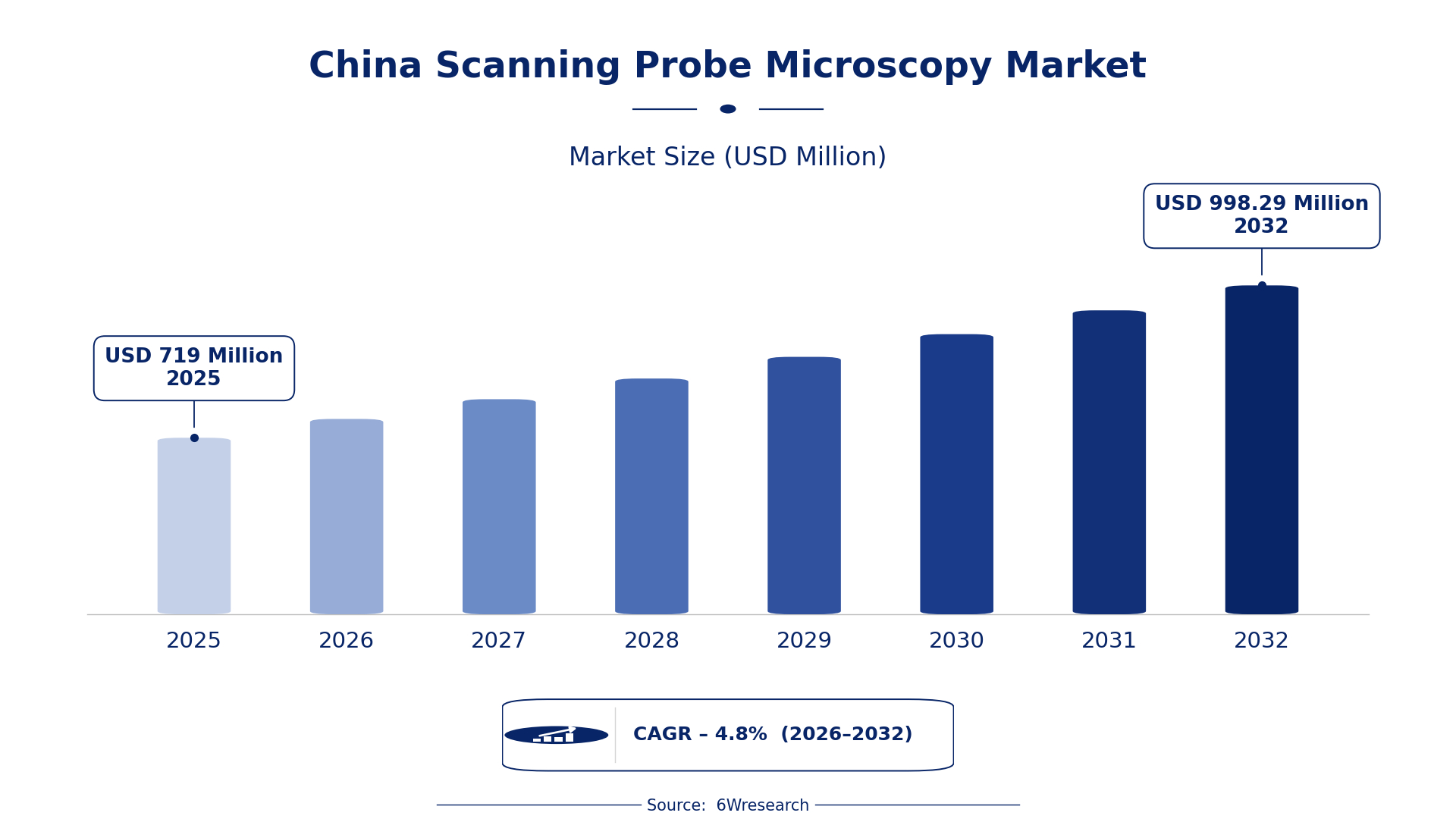
According to 6Wresearch internal database and industry insights, the China Scanning Probe Microscopy Market was valued at USD 719.0 million in 2025 and is projected to reach USD 998.29 million by 2032, growing at a CAGR of approximately 4.8% during 2026–2032.
China Scanning Probe Microscopy Market Highlights
| Report Metric | Details |
| Report Name | China Scanning Probe Microscopy Market |
| Market Size 2025 | USD 719.0 million |
| Market Size 2032 | USD 998.29 million |
| Absolute Growth 2025–2032 | USD 279.29 million |
| CAGR 2026–2032 | 4.8% |
| Peak Annual Growth | 7.2% in 2027 |
| Forecast Period | 2026–2032 |
| Historical Data | 2022–2025 |
| Base Year | 2025 |
| Leading Technique Type, 2025 | AFM (Atomic Force) (53% share) |
| Leading Resolution Level, 2025 | Nanoscale (42% share) |
| Leading Instrument Format, 2025 | Desktop Benchtop (45% share) |
| Leading End User, 2025 | University Research Labs (47% share) |
| Fastest-Growing Technique Type | STM (Scanning Tunneling) (5.8% CAGR) |
| Fastest-Growing Resolution Level | Sub-nanometer (6.2% CAGR) |
| Fastest-Growing Instrument Format | Modular Instruments (7.3% CAGR) |
| Fastest-Growing End User | Nanotech Companies (6.4% CAGR) |
| Growing Sector | Semiconductor R&D |
| Key End Users | University Research Labs, Nanotech Companies, Semiconductor R&D, Materials Science Institutes |
China Scanning Probe Microscopy Market Year-wise Growth Rate and Key Drivers (2022–2032)
This graph illustrates the annual growth rates of the market from 2022 to 2032, highlighting a steady upward trajectory and projected market expansion over the forecast period.
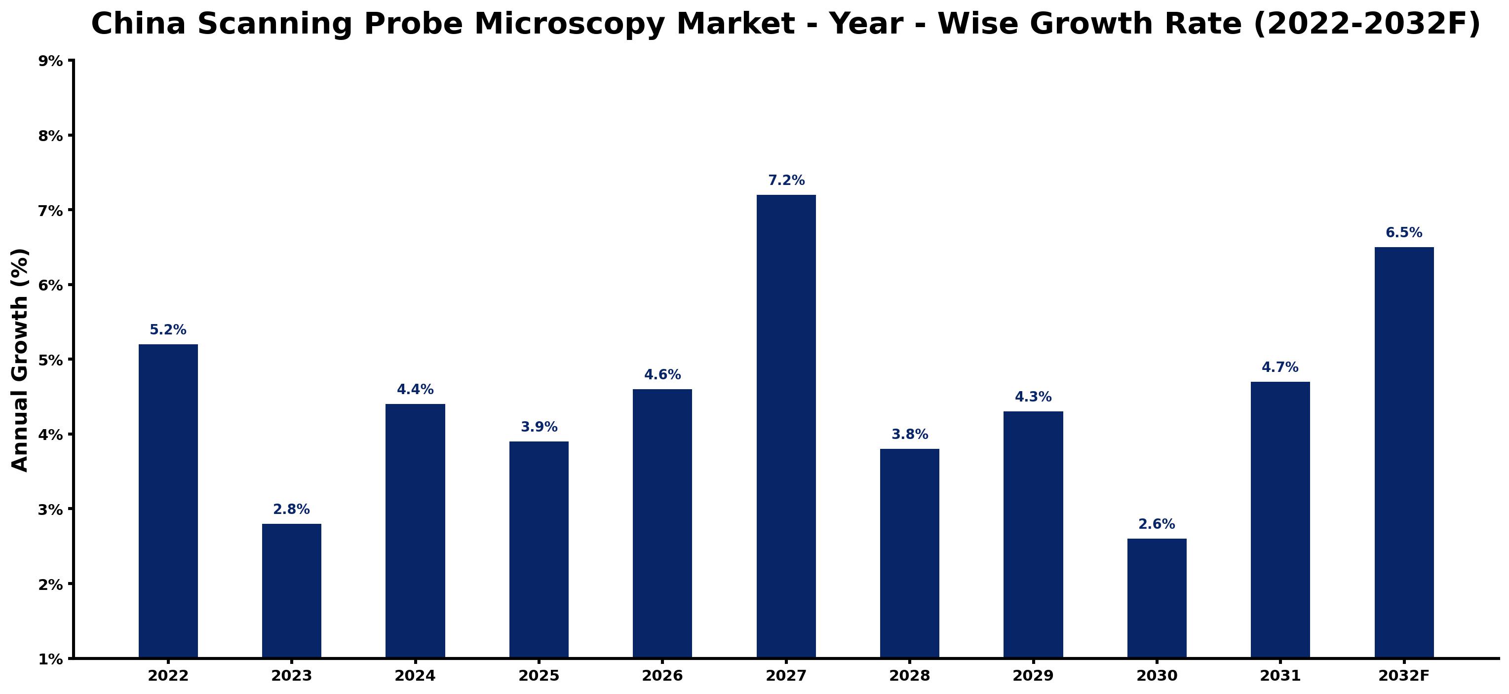
Each row of the following table gives one year's estimated growth and the event or demand shift that explains it.
| Year | Estimated Annual Growth (%) | Market Rationale |
| 2022 | 5.2 | The market experienced steady growth due to increased interest in nanotechnology research. |
| 2023 | 2.8 | Growth slowed as universities adjusted funding priorities for research projects. |
| 2024 | 4.4 | Investment in semiconductor R&D led to faster growth in demand for SPM. |
| 2025 | 3.9 | Demand remained strong, but growth slowed as the market matured. |
| 2026 | 4.6 | Investment in advanced manufacturing technologies spurred growth in SPM applications. |
| 2027 | 7.2 | The market peaked as semiconductor companies ramped up R&D efforts. |
| 2028 | 3.8 | Growth slowed as the market began to stabilise after rapid expansion. |
| 2029 | 4.3 | Increased funding for nanotechnology research revitalised growth in SPM. |
| 2030 | 2.6 | Growth slowed as the market adjusted to new technological standards. |
| 2031 | 4.7 | Demand for SPM instruments increased as research institutions expanded. |
| 2032 | 6.5 | Growth accelerated as new applications in materials science emerged. |
Note: Market size estimations and growth projections presented in this report are based on 6Wresearch's proprietary forecasting methodology, utilizing the latest available industry data, government publications, and primary research inputs.
China Scanning Probe Microscopy Market Synopsis
Scanning Probe Microscopy Market in China encompasses advanced imaging technology used for nanoscale analysis. This technology is crucial for materials characterization, semiconductor development, and nanotechnology research. The market is expanding due to substantial investments in semiconductor R&D and nanotechnology initiatives. With over 200 universities engaged in related research, demand is anticipated to increase. The Chinese government's support through funding and strategic programs further propels this growth.
Market Dynamics Impact Analysis (2026–2032)
| Factor | Type | Impact | Primary Segment Affected |
| Investment in semiconductor R&D | Driver | High | Semiconductor R&D |
| Increasing number of nanotechnology research projects | Driver | High | University Research Labs |
| Emerging applications in materials science | Opportunity | High | Materials Science Institutes |
| Growing demand for advanced microscopy techniques | Opportunity | High | Nanotech Companies |
| High cost of advanced SPM instruments | Restraint | High | Desktop Benchtop |
| Limited awareness of SPM capabilities among new users | Restraint | Medium | University Research Labs |
| Scanning Probe Microscopy Market in China faces high equipment costs | Challenge | High | UHV Chamber Setup |
| Technological advancements require continuous investment in training | Challenge | Medium | Modular Instruments |
Evaluation of Drivers in China Scanning Probe Microscopy Market (2026–2032)
The table below links each growth driver to the segment it affects and the evidence for it.
| Drivers | Primary Segment Affected | Why It Matters (Evidence) |
| Increased funding for semiconductor research | Semiconductor R&D | The Chinese semiconductor industry is projected to invest $150 billion in R&D by 2025, driving demand for SPM instruments. |
| Expansion of nanotechnology programs in universities | University Research Labs | China has over 200 universities with active nanotechnology research programs, increasing the need for SPM. |
| Growing emphasis on advanced materials research | Materials Science Institutes | The National Natural Science Foundation of China funds over 500 SPM-related projects annually, boosting demand. |
| Rising applications of SPM in various industries | Nanotech Companies | Nanoscale imaging is critical for over 50% of semiconductor R&D projects in China, enhancing SPM usage. |
| Development of new SPM techniques | Desktop Benchtop | In 2023, advancements in SPM techniques reported by the Shanghai Institute of Microsystem and Information Technology increased interest. |
The Chinese semiconductor industry will invest $150 billion in R&D by 2025, driving demand for SPM instruments. Over 200 universities are actively engaged in nanotechnology research, increasing the need for advanced microscopy techniques. Recent advancements reported in 2023 have sparked interest in new SPM techniques, contributing to market growth. The National Natural Science Foundation of China funds numerous SPM-related projects annually, boosting usage in materials science and technology development.
Evaluation of Restraints in China Scanning Probe Microscopy Market
The table below lists the restraints and the evidence behind each.
| Market Restraint | Primary Segment Affected | Why It Matters (Evidence) |
| High cost of advanced SPM instruments | Desktop Benchtop | The price of advanced SPM instruments can exceed $100,000, limiting accessibility for smaller labs. |
| Limited awareness of SPM capabilities among new users | University Research Labs | Many new researchers lack knowledge about SPM, hindering adoption in emerging labs. |
| Dependence on skilled technicians for operation | UHV Chamber Setup | The need for highly skilled technicians to operate SPM systems can delay project timelines. |
| Complexity of SPM techniques | Modular Instruments | The intricate nature of SPM techniques can deter potential users from investing in the technology. |
| Regulatory compliance requirements | Nanotech Companies | Manufacturers must meet ISO 9001 certification, adding to operational costs. |
China Scanning Probe Microscopy Market Challenges
The China Scanning Probe Microscopy market faces a critical supply issue stemming from reliance on imported components, which can delay production timelines for manufacturers. This dependency results in lead times extending up to six months for essential parts, impacting producers' ability to meet the growing domestic demand. Technological advancements are hindered by insufficient local innovation in SPM techniques, forcing buyers to rely on outdated equipment that cannot compete with international standards. High costs burden buyers, with over 30% of their budgets allocated to equipment maintenance and upgrades, straining their financial resources. A skills gap exists as the rapid growth in nanotechnology outpaces the training of qualified personnel, limiting the operational capacity of labs and institutes across the country.
Trends in the China Scanning Probe Microscopy Market
Four trends stand out in the China Scanning Probe Microscopy Market.
- Shift from Traditional to Advanced SPM Techniques: In 2023, advancements in SPM techniques reported by the Shanghai Institute of Microsystem and Information Technology have led to increased adoption. This shift is reflected as more research labs seek to implement these advanced methods for better precision.
- Emergence of Nanoscale Imaging in Semiconductor R&D: Since 2021, the focus on nanoscale imaging has intensified within semiconductor R&D projects, with over 50% of projects relying on SPM. This trend highlights the growing need for precision in semiconductor manufacturing.
- Increased Collaboration in Nanotechnology Research: The National Institute of Standards and Technology (NIST) has collaborated with Chinese institutions on SPM standardization efforts since 2022. This partnership improves the quality and reliability of SPM technologies.
- Growth of University Research Labs: In 2022, China had over 200 universities with active nanotechnology research programs. This growth indicates a rising demand for SPM instruments in academic settings.
Investment Opportunities in the China Scanning Probe Microscopy Market
Investors looking at the China Scanning Probe Microscopy Market should consider the following areas.
- $150 Billion Investment in Semiconductor R&D: The Chinese semiconductor industry is set to invest $150 billion by 2025, creating opportunities for suppliers of SPM instruments. Collaborating with semiconductor firms can improve market presence.
- Growing Demand from Nanotech Companies: Nanotech companies are increasingly seeking advanced microscopy solutions, with a projected growth rate of 6.4% in the coming years. Suppliers can enter this market by forming partnerships with leading firms.
- Expansion of University Research Labs: With over 200 universities engaged in nanotechnology research, there is a strong opportunity to supply SPM instruments. Establishing local partnerships can facilitate market entry.
- Emerging Applications in Materials Science: As materials science institutes expand their research capabilities, the demand for SPM instruments is expected to rise. Targeting these institutes can provide a lucrative entry point.
Government Initiatives in the China Scanning Probe Microscopy Market
The Ministry of Science and Technology initiated the 'National Key R&D Program' in 2021, aiming to support nanotechnology capabilities with a budget of $3 billion. This program encourages research and development in advanced microscopy techniques, benefiting producers and buyers alike. Furthermore, the State Council introduced the '14th Five-Year Plan for Scientific and Technological Innovation' in 2022, promoting advanced manufacturing, including SPM technologies. This strategic plan outlines funding priorities and encourages innovation in the sector. Additionally, the National Innovation-Driven Development Strategy established in 2020 supports research in nanotechnology and materials science, facilitating collaboration and technological advancements.
Buyers in university research labs can benefit from the funding allocated by the Ministry of Education's initiative to support nanotechnology research, which announced $500 million in 2023. This funding enables universities to acquire advanced SPM instruments and improve their research capabilities. Furthermore, the National Natural Science Foundation of China has updated its funding guidelines to prioritise projects involving advanced microscopy techniques, ensuring that researchers have access to the latest technologies. This support stimulates innovation and enhances the overall research environment in the country.
Future Insight of the China Scanning Probe Microscopy Market
In the China Scanning Probe Microscopy market, buyers and suppliers can expect transformative changes by 2032 driven by increased investment in R&D, particularly from the semiconductor sector, projected to invest $150 billion in R&D by 2025. The National Key R&D Program will stimulate innovation in nanotechnology, improving the capabilities of SPM instruments. Collaboration with international standards organizations will elevate the quality and reliability of SPM techniques. With over 200 universities engaged in nanotechnology research, the market will benefit from a steady influx of new talent and ideas, creating opportunities for suppliers.
Market Segmentation Analysis
The report offers a comprehensive study of the following market segments and their leading categories in the market.
By Technique Type – AFM (Atomic Force) Dominated, STM (Scanning Tunneling) Expected to Grow Fastest
According to Shubham Padhi, Research Analyst at 6Wresearch, the largest technique type category in 2025 was AFM (Atomic Force), with a 53% share of total revenue. AFM holds the largest market share due to its extensive application in surface topography measurements, which are essential for various research projects. Many of the over 200 universities in China utilise AFM in their nanotechnology research, driving its widespread adoption. Over 2026–2032, STM (Scanning Tunneling) is expected to post the fastest growth, at a CAGR of 5.8%. STM is witnessing rapid growth as it is crucial for studying conductive materials at the atomic level, particularly in semiconductor applications. The projected $150 billion investment in semiconductor R&D by 2025 will further boost the demand for STM technology. This trend indicates that suppliers should enhance their AFM offerings while also investing in STM capabilities to meet the increasing research demands.
By Resolution Level – Nanoscale Dominated, Sub-nanometer Expected to Grow Fastest
Nanoscale took a 42% share of resolution level in 2025, more than any other category. Nanoscale resolution leads the market as it is fundamental for nanotechnology, enabling detailed analyses of materials. This is particularly significant in China's semiconductor industry, where nanoscale imaging is critical for over 50% of R&D projects. Sub-nanometer is set to record the highest CAGR in this split, 6.2% over 2026–2032. Sub-nanometer resolution is rapidly gaining traction due to its vital role in advanced materials science, where precision is increasingly required. The complexity of materials being studied is driving the need for higher resolution techniques. Suppliers should prioritise the development of sub-nanometer solutions to cater to the advancing requirements of research applications.
By Instrument Format – Desktop Benchtop Dominated, Modular Instruments Expected to Grow Fastest
With a 45% revenue share in 2025, Desktop Benchtop was the largest instrument format category. Desktop Benchtop systems dominate the market because they are widely adopted in research labs, offering ease of use and accessibility for a variety of applications. These instruments are particularly favoured in university settings where hands-on experimentation is essential. Modular Instruments are projected to grow fastest, at a CAGR of 7.3% during 2026–2032. Modular Instruments are experiencing the fastest growth as they allow for customised research setups tailored to specific experimental needs. The flexibility of modular systems aligns well with the diverse requirements of modern research environments. This shift suggests that suppliers should focus on providing modular options to attract a broader range of research customers.
By End User – University Research Labs Dominated, Nanotech Companies Expected to Grow Fastest
University Research Labs held a 47% share of the China Scanning Probe Microscopy Market by end user in 2025. University Research Labs command the largest share as they are major users of SPM for various research projects, supported by funding from institutions like the National Natural Science Foundation of China. The presence of over 200 universities with active nanotechnology programs underlines this trend. The quickest growth will come from Nanotech Companies, forecast to expand at a CAGR of 6.4% between 2026 and 2032. Nanotech Companies are the fastest-growing end user group, utilising SPM for product development in a rapidly advancing field. As the demand for nanotechnology solutions increases, these companies will drive further growth in SPM adoption. Suppliers should strategically target nanotech companies to capitalise on the increasing demand for advanced SPM applications.
Key Attractiveness of the Report
- 10 Years of Market Numbers
- Historical Data Starting from 2022 to 2025
- Base Year 2025
- Forecast Data until 2032
- Key Performance Indicators Impacting the Market
- Major Upcoming Developments and Projects
Key Highlights of the Report:
- China Scanning Probe Microscopy Market Outlook
- Market Size of China Scanning Probe Microscopy Market, 2025
- Forecast of China Scanning Probe Microscopy Market, 2032
- Historical Data and Forecast of China Scanning Probe Microscopy Revenues & Volume for the Period 2022 - 2032F
- China Scanning Probe Microscopy Market Trend Evolution
- China Scanning Probe Microscopy Market Drivers and Challenges
- China Scanning Probe Microscopy Price Trends
- China Scanning Probe Microscopy Porter's Five Forces
- China Scanning Probe Microscopy Industry Life Cycle
- Historical Data and Forecast of China Scanning Probe Microscopy Market Revenues & Volume By Technique Type for the Period 2022 - 2032F
- Historical Data and Forecast of China Scanning Probe Microscopy Market Revenues & Volume By AFM (Atomic Force) for the Period 2022 - 2032F
- Historical Data and Forecast of China Scanning Probe Microscopy Market Revenues & Volume By STM (Scanning Tunneling) for the Period 2022 - 2032F
- Historical Data and Forecast of China Scanning Probe Microscopy Market Revenues & Volume By Magnetic Force Microscopy for the Period 2022 - 2032F
- Historical Data and Forecast of China Scanning Probe Microscopy Market Revenues & Volume By Near-Field Scanning Optical for the Period 2022 - 2032F
- Historical Data and Forecast of China Scanning Probe Microscopy Market Revenues & Volume By Resolution Level for the Period 2022 - 2032F
- Historical Data and Forecast of China Scanning Probe Microscopy Market Revenues & Volume By Nanoscale for the Period 2022 - 2032F
- Historical Data and Forecast of China Scanning Probe Microscopy Market Revenues & Volume By Atomic-scale for the Period 2022 - 2032F
- Historical Data and Forecast of China Scanning Probe Microscopy Market Revenues & Volume By Sub-nanometer for the Period 2022 - 2032F
- Historical Data and Forecast of China Scanning Probe Microscopy Market Revenues & Volume By Near-field for the Period 2022 - 2032F
- Historical Data and Forecast of China Scanning Probe Microscopy Market Revenues & Volume By Instrument Format for the Period 2022 - 2032F
- Historical Data and Forecast of China Scanning Probe Microscopy Market Revenues & Volume By Desktop Benchtop for the Period 2022 - 2032F
- Historical Data and Forecast of China Scanning Probe Microscopy Market Revenues & Volume By UHV Chamber Setup for the Period 2022 - 2032F
- Historical Data and Forecast of China Scanning Probe Microscopy Market Revenues & Volume By Modular Instruments for the Period 2022 - 2032F
- Historical Data and Forecast of China Scanning Probe Microscopy Market Revenues & Volume By Enclosed Benchtop for the Period 2022 - 2032F
- Historical Data and Forecast of China Scanning Probe Microscopy Market Revenues & Volume By End User for the Period 2022 - 2032F
- Historical Data and Forecast of China Scanning Probe Microscopy Market Revenues & Volume By University Research Labs for the Period 2022 - 2032F
- Historical Data and Forecast of China Scanning Probe Microscopy Market Revenues & Volume By Nanotech Companies for the Period 2022 - 2032F
- Historical Data and Forecast of China Scanning Probe Microscopy Market Revenues & Volume By Semiconductor R&D for the Period 2022 - 2032F
- Historical Data and Forecast of China Scanning Probe Microscopy Market Revenues & Volume By Materials Science Institutes for the Period 2022 - 2032F
- China Scanning Probe Microscopy Import Export Trade Statistics
- Market Opportunity Assessment By Technique Type
- Market Opportunity Assessment By Resolution Level
- Market Opportunity Assessment By Instrument Format
- Market Opportunity Assessment By End User
- China Scanning Probe Microscopy Top Companies Market Share
- China Scanning Probe Microscopy Competitive Benchmarking By Technical and Operational Parameters
- China Scanning Probe Microscopy Company Profiles
- China Scanning Probe Microscopy Key Strategic Recommendations
Market Covered
Segments analysed in this report are listed below.
By Technique Type
- AFM (Atomic Force)
- STM (Scanning Tunneling)
- Magnetic Force Microscopy
- Near-Field Scanning Optical
By Resolution Level
- Nanoscale
- Atomic-scale
- Sub-nanometer
- Near-field
By Instrument Format
- Desktop Benchtop
- UHV Chamber Setup
- Modular Instruments
- Enclosed Benchtop
By End User
- University Research Labs
- Nanotech Companies
- Semiconductor R&D
- Materials Science Institutes