China Semiconductor Inspection Market Size & Growth Rate
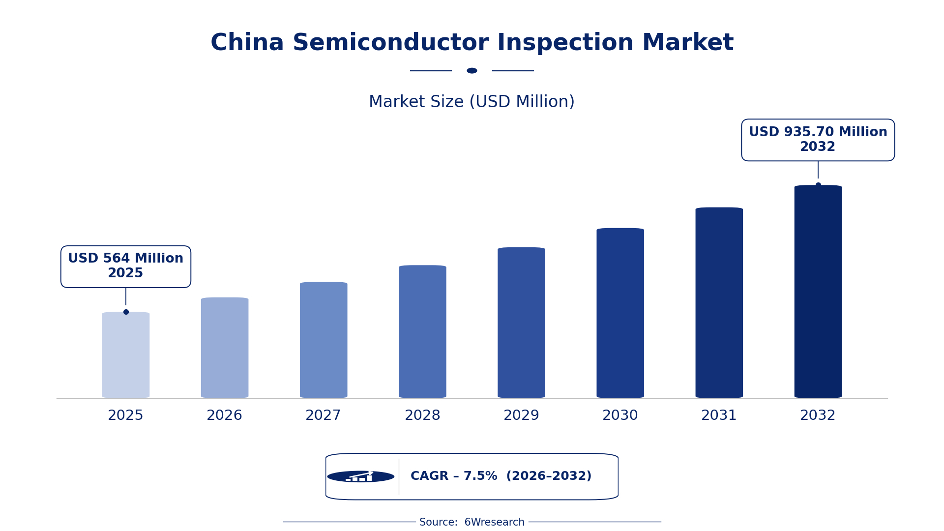
According to 6Wresearch internal database and industry insights, the China Semiconductor Inspection Market was valued at USD 564.0 million in 2025 and is projected to reach USD 935.70 million by 2032, growing at a CAGR of approximately 7.5% during 2026–2032.
China Semiconductor Inspection Market Highlights
| Report Metric | Details |
| Report Name | China Semiconductor Inspection Market |
| Market Size 2025 | USD 564.0 million |
| Market Size 2032 | USD 935.70 million |
| Absolute Growth 2025–2032 | USD 371.70 million |
| CAGR 2026–2032 | 7.5% |
| Peak Annual Growth | 9.5% in 2028 |
| Forecast Period | 2026–2032 |
| Historical Data | 2022–2025 |
| Base Year | 2025 |
| Leading Inspection Type, 2025 | Wafer Inspection (44% share) |
| Leading Stage of Inspection, 2025 | Post-Deposition (54% share) |
| Leading Technology Used, 2025 | Optical + e-Beam (38% share) |
| Leading End User, 2025 | Foundries & IDMs (50% share) |
| Fastest-Growing Inspection Type | Defect Review Systems (9.4% CAGR) |
| Fastest-Growing Stage of Inspection | Pre-Lithography (9.3% CAGR) |
| Fastest-Growing Technology Used | AI + Machine Vision (9.1% CAGR) |
| Fastest-Growing End User | OSATs (9.3% CAGR) |
| Growing Sector | Semiconductor Manufacturing |
| Key End Users | Foundries, IDMs, OSATs, Photomask Makers |
China Semiconductor Inspection Market Year-wise Growth Rate and Key Drivers (2022–2032)
This graph illustrates the annual growth rates of the market from 2022 to 2032, highlighting a steady upward trajectory and projected market expansion over the forecast period.
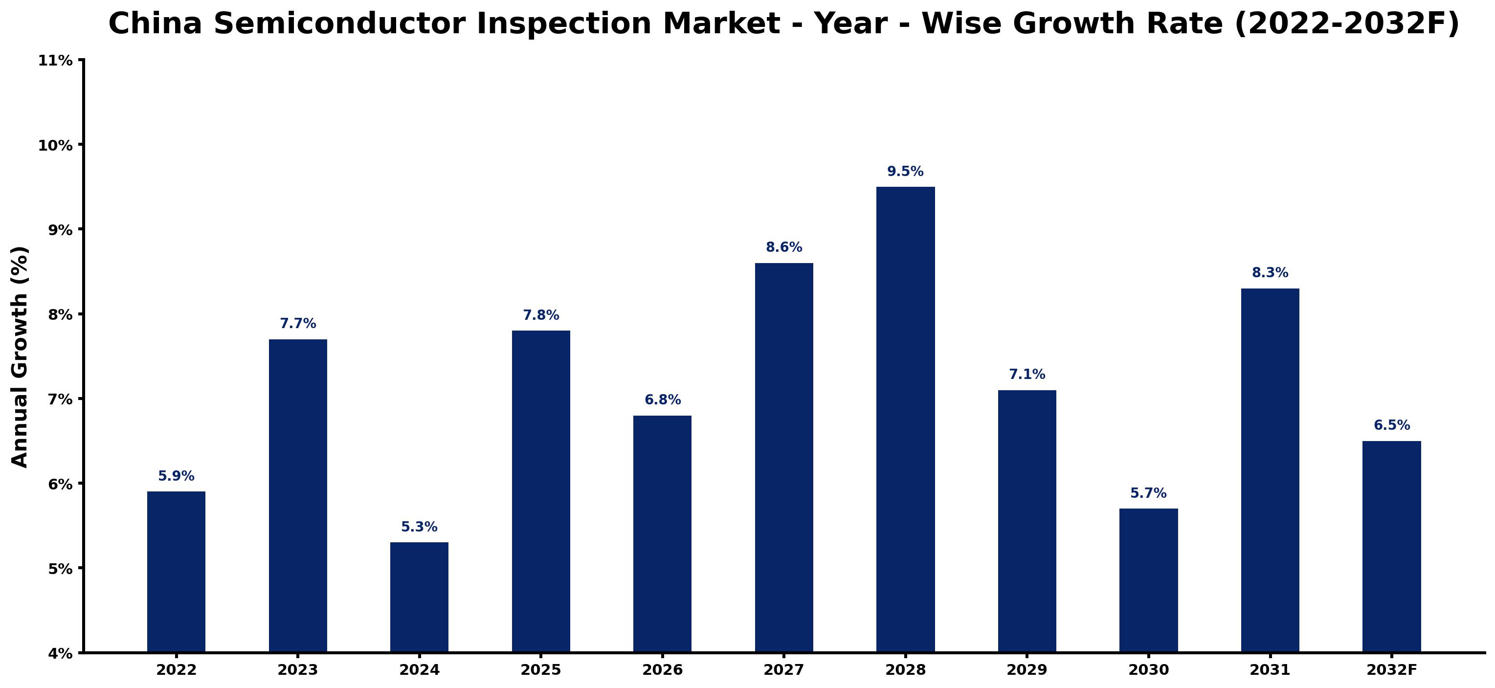
The following table presents the estimated annual growth rate for each year together with the principal factor influencing market performance.
| Year | Estimated Annual Growth (%) | Market Rationale |
| 2022 | 5.9 | The market experienced steady growth due to increased domestic demand for semiconductors. |
| 2023 | 7.7 | Growth accelerated as investments in semiconductor technology expanded manufacturing capabilities. |
| 2024 | 5.3 | A slowdown occurred as the market adjusted to previous rapid growth rates. |
| 2025 | 7.8 | Growth rebounded, driven by significant investments in advanced semiconductor technologies. |
| 2026 | 6.8 | The market growth slowed as manufacturers focused on optimising existing processes. |
| 2027 | 8.6 | Demand surged as new technologies were adopted in semiconductor manufacturing. |
| 2028 | 9.5 | The peak growth rate was achieved, reflecting strong investment and demand. |
| 2029 | 7.1 | Growth slowed as the market matured and demand stabilised. |
| 2030 | 5.7 | A further slowdown occurred as the market adjusted to previous peaks. |
| 2031 | 8.3 | Growth picked up again, driven by innovation in semiconductor inspection technologies. |
| 2032 | 6.5 | The market continues to grow, albeit at a slower rate, as competition intensifies. |
Note: Market size estimations and growth projections presented in this report are based on 6Wresearch's proprietary forecasting methodology, utilizing the latest available industry data, government publications, and primary research inputs.
China Semiconductor Inspection Market Synopsis
Semiconductor Inspection in China focuses on evaluating the quality and integrity of semiconductor materials through advanced technologies. This process is crucial for ensuring the reliability of electronic chips and optimising manufacturing. The China Semiconductor Inspection Market is expanding due to rising domestic demand, substantial investments in technology, and government initiatives such as the 'Made in China 2025' programme. By 2030, the semiconductor industry is expected to reach $1 trillion, indicating a promising future for inspection technologies.
Market Dynamics Impact Analysis (2026–2032)
| Factor | Type | Impact | Primary Segment Affected |
| Increased investment in semiconductor manufacturing capabilities | Driver | High | Wafer Inspection |
| Growing demand for high-quality semiconductor devices | Driver | High | Die Inspection |
| Rising need for advanced inspection technologies | Opportunity | High | Defect Review Systems |
| Expansion of semiconductor manufacturing facilities in key regions | Opportunity | High | Post-Deposition |
| Limited availability of skilled workforce in semiconductor inspection | Restraint | Medium | Mask Inspection |
| High costs associated with advanced inspection equipment | Restraint | Medium | Pre-Packaging |
| Buyers face challenges in sourcing reliable inspection technologies | Challenge | High | Across Nodes |
| Suppliers struggle with rapid technological advancements in inspection methods | Challenge | Medium | AI + Machine Vision |
Evaluation of Drivers in China Semiconductor Inspection Market (2026–2032)
The table below links each growth driver to the segment it affects and the evidence for it.
| Drivers | Primary Segment Affected | Why It Matters (Evidence) |
| Increased investment in semiconductor manufacturing capabilities | Wafer Inspection | China's semiconductor industry is projected to reach $1 trillion by 2030, driving demand for inspection technologies. |
| Growing demand for high-quality semiconductor devices | Die Inspection | China's population of over 1.4 billion fuels demand for electronic devices, increasing the need for reliable chips. |
| Expansion of semiconductor manufacturing facilities in key regions | Post-Deposition | The Shanghai region hosts numerous fabs, increasing the need for advanced inspection technologies to ensure quality. |
| Rising need for advanced inspection technologies | Defect Review Systems | The government aims for 70% domestic semiconductor production by 2025, necessitating quality control and inspection. |
| Focus on optimising manufacturing processes | Pre-Packaging | The installed base of semiconductor inspection equipment was estimated at 15,000 units in 2022, indicating strong market potential. |
Market growth in China for Semiconductor Inspection rests on increased investment in semiconductor manufacturing capabilities, driven by a projected industry value of $1 trillion by 2030. The demand for high-quality semiconductor devices arises from a population exceeding 1.4 billion, leading to more electronic purchases. Expansion of manufacturing facilities boosts the need for inspection technologies, particularly in the Shanghai region. The target of 70% domestic production by 2025 further fuels demand for advanced inspection methods. The installed base of semiconductor inspection equipment was estimated at 15,000 units in 2022, indicating a strong market foundation.
Evaluation of Restraints in China Semiconductor Inspection Market
The table below lists the restraints and the evidence behind each.
| Market Restraint | Primary Segment Affected | Why It Matters (Evidence) |
| Limited availability of skilled workforce in semiconductor inspection | Mask Inspection | The shortage of skilled professionals hampers the implementation of advanced inspection technologies, affecting production efficiency. |
| High costs associated with advanced inspection equipment | Pre-Packaging | The investment required for equipment limits accessibility for smaller manufacturers, impacting their operational capabilities. |
| Challenges in sourcing reliable inspection technologies | Across Nodes | The rapid pace of technological advancements creates difficulties in finding suitable inspection solutions for manufacturers. |
| Suppliers struggle with rapid technological advancements in inspection methods | AI + Machine Vision | Keeping up with innovations requires constant investment and adaptation from suppliers, straining their resources. |
| Regulatory compliance can delay equipment approval processes | Defect Review Systems | Stringent standards can prolong the time to market for new inspection technologies, affecting competitiveness. |
China Semiconductor Inspection Market Challenges
Buyers in the China Semiconductor Inspection Market face regulatory challenges due to the National Standard GB/T 29862-2013, which raises compliance costs by approximately 15% for manufacturers. Intense competition among over 1,000 semiconductor companies results in lower prices and tighter profit margins for suppliers. Technology adoption remains limited, with only 15,000 units of semiconductor inspection equipment operational as of 2022, hindering efficiency and innovation for producers. Additionally, rising costs associated with advanced technologies strain budgets and delay project timelines for both buyers and suppliers, complicating their operational strategies.
Trends in the China Semiconductor Inspection Market
Buyers and suppliers in the China Semiconductor Inspection Market are adjusting to the following trends.
- Shift towards AI and Machine Vision in Inspection: The semiconductor inspection market is increasingly adopting AI and machine vision technologies, improving defect detection capabilities. In 2023, this shift is expected to grow by 9.1%, reflecting the industry's push for automation and efficiency.
- Transition from Optical to Advanced Inspection Technologies: Since 2022, there has been a notable move from traditional optical methods to more advanced techniques like e-beam inspection. This change is driven by the need for higher precision in semiconductor manufacturing processes.
- Emergence of Post-Deposition Inspection as a Key Focus: Post-Deposition inspection has gained prominence since 2021, with a focus on ensuring quality after deposition processes. This segment is projected to grow as manufacturers seek to enhance product reliability and performance.
- Increased Collaboration between Foundries and Inspection Providers: Foundries and inspection technology providers have strengthened partnerships since 2022, leading to improved inspection solutions. This collaboration is vital for meeting the growing demands of semiconductor production and ensuring quality.
Investment Opportunities in the China Semiconductor Inspection Market
Some of the investment opportunities in the China Semiconductor Inspection Market are mentioned below.
- Foundries seeking advanced inspection solutions: With the semiconductor market projected to reach $1 trillion by 2030, foundries require advanced inspection technologies to maintain quality. Collaborating with local partners can facilitate entry into this expanding market and improve production capabilities.
- Investment opportunities in semiconductor technology development: The recent approval of a $10 billion investment plan in 2023 presents a valuable opportunity for suppliers. Engaging with the Semiconductor Industry Association of China can pave the way for new partnerships and technology advancements.
- Rising demand for defect review systems: As semiconductor manufacturing grows, the demand for defect review systems is on the rise. Suppliers can enter this market by forming joint ventures with local manufacturers to meet quality standards.
- Emerging need for pre-packaging inspection technologies: The increasing emphasis on quality before packaging creates opportunities for suppliers. Establishing certification with relevant authorities can facilitate market entry and ensure compliance with industry standards.
Government Initiatives in the China Semiconductor Inspection Market
The 'Made in China 2025' initiative prioritises semiconductor technology, aiming for 70% domestic production by 2025. This policy encourages local manufacturers to invest in advanced inspection technologies, ensuring compliance with national standards. The initiative supports the growth of the semiconductor inspection market by promoting innovation and enhancing production capabilities. Furthermore, the '14th Five-Year Plan for the Integrated Circuit Industry' launched in 2021 reinforces these goals, driving investments in manufacturing and inspection processes. The National Semiconductor Innovation Fund, established in 2022 with a budget of $5 billion, supports research and development in semiconductor technologies, further advancing the industry.
In 2023, the Ministry of Industry and Information Technology approved a $10 billion investment plan for semiconductor technology development. This funding aims to enhance semiconductor manufacturing capabilities, including inspection technologies. Additionally, the National Semiconductor Innovation Fund supports research and development in semiconductor technologies, enabling producers to improve their inspection methods. These initiatives are essential for advancing inspection processes and ensuring quality control in semiconductor production.
Future Insight of the China Semiconductor Inspection Market
The China Semiconductor Inspection Market is set to progress by 2032, driven by the government's 'Made in China 2025' initiative, which targets 70% domestic semiconductor production. New government programmes will enhance semiconductor manufacturing capabilities, raising local production standards. Demand for reliable chips will rise as the semiconductor industry is expected to reach $1 trillion by 2030, necessitating more electronic devices. Investment in advanced technologies will optimise inspection processes, providing substantial advantages for both buyers and suppliers.
Market Segmentation Analysis
The analysis below covers each segmentation, its leading category in 2025 and its fastest-growing category through 2032.
By Inspection Type – Wafer Inspection Dominated, Defect Review Systems Expected to Grow Fastest
According to Shubham Padhi, Research Analyst at 6Wresearch, with a 44% revenue share in 2025, Wafer Inspection was the largest inspection type category. Wafer Inspection holds the largest market share as it is vital for quality control in semiconductor manufacturing. This method is particularly significant in regions like Shanghai, which is a major hub for semiconductor production facilities. Defect Review Systems are set to record the highest CAGR in this split, 9.4% over 2026–2032. Defect Review Systems are experiencing rapid growth due to their importance in analysing defects identified during inspections. As the semiconductor industry expands, the need for effective defect analysis will drive further adoption of these systems. Suppliers should enhance defect review technologies to meet the rising demand in the semiconductor inspection market.
By Stage of Inspection – Post-Deposition Dominated, Pre-Lithography Expected to Grow Fastest
In 2025, Post-Deposition led the stage of inspection split with a 54% share. Post-Deposition inspection leads the market as it is essential for verifying layers after deposition processes, ensuring the integrity of semiconductor devices. This stage is particularly critical in advanced fabrication facilities where precision is key. Over 2026–2032, Pre-Lithography is expected to post the fastest growth, at a CAGR of 9.3%. Pre-Lithography inspection is the fastest-growing segment because it is crucial for quality assurance before lithography, a significant phase in semiconductor fabrication. As manufacturers strive for higher yields, the emphasis on pre-lithography checks will increase substantially. Suppliers must focus on advancing pre-lithography inspection technologies to capitalise on this growth opportunity.
By Technology Used – Optical + e-Beam Dominated, AI + Machine Vision Expected to Grow Fastest
Optical + e-Beam took a 38% share of technology used in 2025, more than any other category. Optical + e-Beam technology dominates the market due to its widespread application in semiconductor inspection, delivering reliable results for manufacturers. These methods are essential for maintaining quality throughout various stages of semiconductor production. AI + Machine Vision is projected to grow fastest, at a CAGR of 9.1% during 2026–2032. AI + Machine Vision technology is rapidly gaining popularity as it provides automated defect detection capabilities, enhancing inspection efficiency. The growing complexity of semiconductor designs necessitates advanced solutions to meet quality standards. This trend indicates that suppliers should invest in AI and machine vision technologies to remain competitive in the semiconductor inspection market.
By End User – Foundries & IDMs Dominated, OSATs Expected to Grow Fastest
Foundries & IDMs accounted for a 50% market share by end user in 2025. Foundries & IDMs hold the largest market share as they are the primary users of inspection technologies, vital for upholding high production standards. Their substantial investments in semiconductor manufacturing drive the demand for effective inspection solutions. The quickest growth will come from OSATs, forecast to expand at a CAGR of 9.3% between 2026 and 2032. OSATs represent the fastest-growing end user segment, relying heavily on inspection for packaging processes. As the demand for packaged semiconductor devices escalates, OSATs will increasingly seek advanced inspection technologies to ensure quality. This indicates that suppliers should tailor their offerings to meet the specific needs of OSATs to capture this expanding market.
Key Attractiveness of the Report
- 10 Years of Market Numbers
- Historical Data Starting from 2022 to 2025
- Base Year 2025
- Forecast Data until 2032
- Key Performance Indicators Impacting the Market
- Major Upcoming Developments and Projects
Key Highlights of the Report:
- China Semiconductor Inspection Market Outlook
- Market Size of China Semiconductor Inspection Market, 2025
- Forecast of China Semiconductor Inspection Market, 2032
- Historical Data and Forecast of China Semiconductor Inspection Revenues & Volume for the Period 2022 - 2032F
- China Semiconductor Inspection Market Trend Evolution
- China Semiconductor Inspection Market Drivers and Challenges
- China Semiconductor Inspection Price Trends
- China Semiconductor Inspection Porter's Five Forces
- China Semiconductor Inspection Industry Life Cycle
- Historical Data and Forecast of China Semiconductor Inspection Market Revenues & Volume By Inspection Type for the Period 2022 - 2032F
- Historical Data and Forecast of China Semiconductor Inspection Market Revenues & Volume By Wafer Inspection for the Period 2022 - 2032F
- Historical Data and Forecast of China Semiconductor Inspection Market Revenues & Volume By Die Inspection for the Period 2022 - 2032F
- Historical Data and Forecast of China Semiconductor Inspection Market Revenues & Volume By Mask Inspection for the Period 2022 - 2032F
- Historical Data and Forecast of China Semiconductor Inspection Market Revenues & Volume By Defect Review Systems for the Period 2022 - 2032F
- Historical Data and Forecast of China Semiconductor Inspection Market Revenues & Volume By Stage of Inspection for the Period 2022 - 2032F
- Historical Data and Forecast of China Semiconductor Inspection Market Revenues & Volume By Post-Deposition for the Period 2022 - 2032F
- Historical Data and Forecast of China Semiconductor Inspection Market Revenues & Volume By Pre-Packaging for the Period 2022 - 2032F
- Historical Data and Forecast of China Semiconductor Inspection Market Revenues & Volume By Pre-Lithography for the Period 2022 - 2032F
- Historical Data and Forecast of China Semiconductor Inspection Market Revenues & Volume By Across Nodes for the Period 2022 - 2032F
- Historical Data and Forecast of China Semiconductor Inspection Market Revenues & Volume By Technology Used for the Period 2022 - 2032F
- Historical Data and Forecast of China Semiconductor Inspection Market Revenues & Volume By Optical + e-Beam for the Period 2022 - 2032F
- Historical Data and Forecast of China Semiconductor Inspection Market Revenues & Volume By SEM/X-ray for the Period 2022 - 2032F
- Historical Data and Forecast of China Semiconductor Inspection Market Revenues & Volume By UV Optical Scanning for the Period 2022 - 2032F
- Historical Data and Forecast of China Semiconductor Inspection Market Revenues & Volume By AI + Machine Vision for the Period 2022 - 2032F
- Historical Data and Forecast of China Semiconductor Inspection Market Revenues & Volume By End User for the Period 2022 - 2032F
- Historical Data and Forecast of China Semiconductor Inspection Market Revenues & Volume By Foundries & IDMs for the Period 2022 - 2032F
- Historical Data and Forecast of China Semiconductor Inspection Market Revenues & Volume By OSATs for the Period 2022 - 2032F
- Historical Data and Forecast of China Semiconductor Inspection Market Revenues & Volume By Photomask Makers for the Period 2022 - 2032F
- Historical Data and Forecast of China Semiconductor Inspection Market Revenues & Volume By Advanced Node Fabs for the Period 2022 - 2032F
- China Semiconductor Inspection Import Export Trade Statistics
- Market Opportunity Assessment By Inspection Type
- Market Opportunity Assessment By Stage of Inspection
- Market Opportunity Assessment By Technology Used
- Market Opportunity Assessment By End User
- China Semiconductor Inspection Top Companies Market Share
- China Semiconductor Inspection Competitive Benchmarking By Technical and Operational Parameters
- China Semiconductor Inspection Company Profiles
- China Semiconductor Inspection Key Strategic Recommendations
Market Covered
This report examines the market across the segments below.
By Inspection Type
- Wafer Inspection
- Die Inspection
- Mask Inspection
- Defect Review Systems
By Stage of Inspection
- Post-Deposition
- Pre-Packaging
- Pre-Lithography
- Across Nodes
By Technology Used
- Optical + e-Beam
- SEM/X-ray
- UV Optical Scanning
- AI + Machine Vision
By End User
- Foundries & IDMs
- OSATs
- Photomask Makers
- Advanced Node Fabs