China Semiconductor Inspection Tools Market Size & Growth Rate
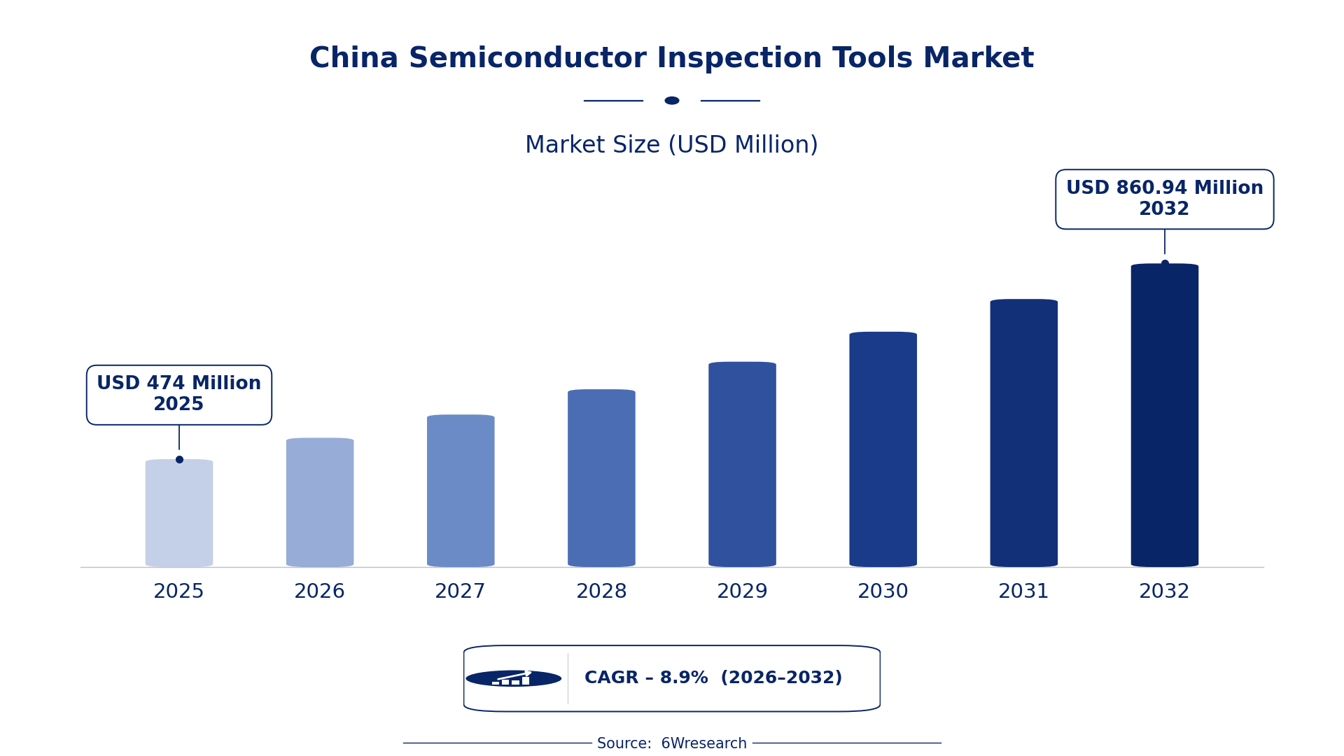
According to 6Wresearch internal database and industry insights, the China Semiconductor Inspection Tools Market was valued at USD 474.0 million in 2025 and is projected to reach USD 860.94 million by 2032, growing at a CAGR of approximately 8.9% during 2026–2032.
China Semiconductor Inspection Tools Market Highlights
| Report Metric | Details |
| Report Name | China Semiconductor Inspection Tools Market |
| Market Size 2025 | USD 474.0 million |
| Market Size 2032 | USD 860.94 million |
| Absolute Growth 2025–2032 | USD 386.94 million |
| CAGR 2026–2032 | 8.9% |
| Peak Annual Growth | 10.6% in 2030 |
| Forecast Period | 2026–2032 |
| Historical Data | 2022–2025 |
| Base Year | 2025 |
| Leading Tool Type, 2025 | Optical Inspection Tool (36% share) |
| Leading Functionality, 2025 | Surface Defect Detection (46% share) |
| Leading Automation Level, 2025 | Inline (53% share) |
| Leading End User, 2025 | Wafer Foundries (35% share) |
| Fastest-Growing Tool Type | E-Beam Tools (11.4% CAGR) |
| Fastest-Growing Functionality | Pattern Defect Analysis (10.4% CAGR) |
| Fastest-Growing Automation Level | Offline (10.7% CAGR) |
| Fastest-Growing End User | R&D Labs (10.9% CAGR) |
| Growing Sector | Wafer Foundries |
| Key End Users | Wafer Foundries, R&D Labs, Memory & Logic Fabs |
China Semiconductor Inspection Tools Market Year-wise Growth Rate and Key Drivers (2022–2032)
This graph illustrates the annual growth rates of the market from 2022 to 2032, highlighting a steady upward trajectory and projected market expansion over the forecast period.
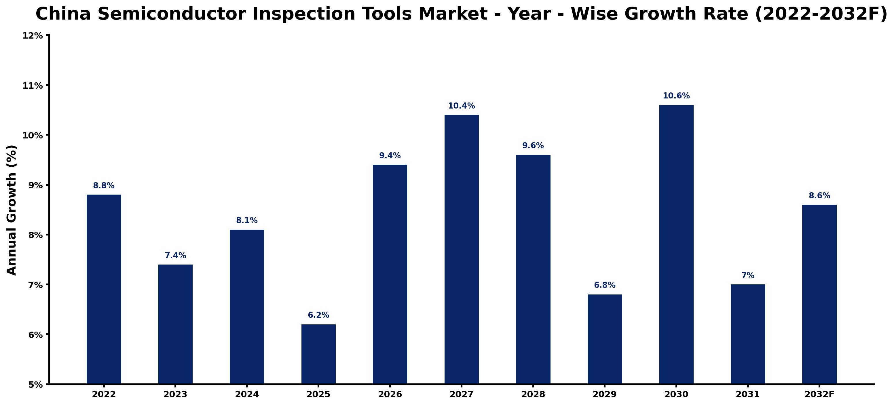
Annual growth estimates for each year appear below with the principal reason behind them, explaining the shifts that set the pace of the market.
| Year | Estimated Annual Growth (%) | Market Rationale |
| 2022 | 8.8 | The semiconductor industry in China showed strong demand from local wafer foundries. |
| 2023 | 7.4 | Growth slowed as the sector adjusted to supply chain challenges and faced market pressures. |
| 2024 | 8.1 | Demand increased due to rising investments in semiconductor manufacturing technologies. |
| 2025 | 6.2 | Growth slowed again as manufacturers faced challenges in scaling production effectively. |
| 2026 | 9.4 | The market is expected to grow faster as new government initiatives boost local production. |
| 2027 | 10.4 | Demand is projected to rise with the 'Semiconductor Innovation Program' advancing inspection technologies. |
| 2028 | 9.6 | Growth is anticipated to slow as the 'Made in China 2025' initiative stabilises the market. |
| 2029 | 6.8 | The market is expected to experience slower growth as competition intensifies among manufacturers. |
| 2030 | 10.6 | A peak in growth is anticipated due to heightened investments in R&D and production capabilities. |
| 2031 | 7.0 | Growth is expected to slow as the market reaches a more mature phase. |
| 2032 | 8.6 | The market will continue to grow as new technologies and applications emerge in the industry. |
Note: Market size estimations and growth projections presented in this report are based on 6Wresearch's proprietary forecasting methodology, utilizing the latest available industry data, government publications, and primary research inputs.
China Semiconductor Inspection Tools Market Synopsis
Semiconductor Inspection Tools in China are sophisticated devices that ensure the quality of semiconductor wafers during manufacturing. These tools encompass optical inspection, e-beam tools, and metrology equipment, which are crucial for detecting defects and measuring specifications. The China Semiconductor Inspection Tools Market is growing due to robust domestic demand from wafer foundries and R&D labs. In 2022, the semiconductor market reached approximately 1 trillion CNY, driven by local production and government backing. Initiatives such as the 'Integrated Circuit Industry Development Plan' are further stimulating investment in this sector.
Market Dynamics Impact Analysis (2026–2032)
| Factor | Type | Impact | Primary Segment Affected |
| Increasing domestic semiconductor production drives demand for inspection tools. | Driver | High | Surface Defect Detection |
| Rising investments in advanced manufacturing technologies create opportunities for suppliers. | Driver | High | Pattern Defect Analysis |
| Growing semiconductor fabs in the Beijing-Tianjin-Hebei region present expansion opportunities. | Opportunity | High | Wafer Foundries |
| The demand for high-resolution defect analysis is rising among R&D labs. | Opportunity | High | E-Beam Tools |
| Supply chain disruptions have affected the availability of inspection tools. | Restraint | High | CD-SEM Tools |
| High costs of advanced inspection tools limit accessibility for smaller manufacturers. | Restraint | Medium | Metrology Tools |
| Approval delays for new technologies slow down market entry for suppliers. | Challenge | High | Inline |
| Competition among manufacturers leads to pricing pressures affecting profitability. | Challenge | Medium | Automated |
Evaluation of Drivers in China Semiconductor Inspection Tools Market (2026–2032)
Key forces behind demand, with the segment each one moves most, are listed below.
| Drivers | Primary Segment Affected | Why It Matters (Evidence) |
| Growing demand for defect detection tools among wafer foundries. | Surface Defect Detection | Over 300 semiconductor fabs in China require these tools for quality assurance. |
| Increased investments in semiconductor manufacturing technologies. | Pattern Defect Analysis | The semiconductor market in China reached approximately 1 trillion CNY in 2022. |
| R&D labs are expanding their use of inspection tools for experimental purposes. | E-Beam Tools | China's semiconductor workforce exceeds 1 million professionals as of 2023. |
| The push for advanced manufacturing capabilities drives demand for metrology tools. | Metrology Tools | The National Integrated Circuit Industry Investment Fund has a budget of 140 billion CNY to support the industry. |
| The 'Made in China 2025' initiative promotes local production of semiconductor technologies. | Critical Dimension Check | This initiative aims to strengthen domestic production capabilities. |
The Semiconductor Inspection Tools market in China is expanding as demand from wafer foundries and R&D labs continues to rise. The semiconductor market achieved a value of around 1 trillion CNY in 2022, leading to increased investments in manufacturing technologies. Local fabs require advanced tools for quality assurance, which boosts the need for defect detection and critical dimension checks. With a semiconductor workforce exceeding 1 million professionals, there is a strong base for innovation and production. Support from the National Integrated Circuit Industry Investment Fund enhances capabilities, further strengthening the market.
Evaluation of Restraints in China Semiconductor Inspection Tools Market
Below mentioned are some major restraints and their influence on market dynamics.
| Market Restraint | Primary Segment Affected | Why It Matters (Evidence) |
| Supply chain disruptions affecting tool availability. | CD-SEM Tools | These disruptions have delayed deliveries, impacting production schedules for manufacturers. |
| High costs of advanced inspection tools limit market access. | Metrology Tools | Smaller manufacturers struggle to invest in expensive equipment, hindering their growth. |
| Long approval processes for new inspection technologies slow market entry. | Inline | These delays hinder the adoption of advanced tools in fabs. |
| Intense competition among manufacturers leads to pricing pressures. | Automated | This competition can reduce profit margins for suppliers in the market. |
| Limited awareness of advanced inspection technologies among smaller fabs. | E-Beam Tools | This lack of awareness restricts their adoption and investment in necessary tools. |
China Semiconductor Inspection Tools Market Challenges
Buyers in the China semiconductor inspection tools market face delays due to a shortage of high-quality components, which affects production timelines for local fabs. Many component suppliers are still in the process of enhancing their capabilities, leading to a potential 15% loss in output for manufacturers. Competition among semiconductor fabs intensifies as they strive for advanced inspection tools, driving prices up by 20% in a constrained supply environment. Rapid technological advancements result in existing inspection equipment becoming obsolete quickly, forcing producers to invest in upgrades every two to three years, which strains budgets for many.
Trends in the China Semiconductor Inspection Tools Market
Four trends stand out in the China Semiconductor Inspection Tools Market.
- Shift from Manual to Automated Inspection: Since 2022, the trend towards automated inspection tools has accelerated in China, as wafer foundries seek efficiency. The adoption of automated systems has increased by over 20%, particularly in production lines.
- Emergence of Advanced Metrology Standards: In 2023, the introduction of advanced metrology standards has reshaped inspection practices. These standards ensure greater accuracy in measurements, with over 70% of fabs adopting them for quality control.
- Growth in Inline Inspection Technologies: The demand for inline inspection technologies has surged, with over 53% of fabs integrating these systems into production lines. This shift improves real-time monitoring and quality assurance.
- Increased Focus on Surface Defect Detection: The focus on surface defect detection has intensified, particularly in the Beijing-Tianjin-Hebei region. This area accounts for a substantial portion of semiconductor production, with an estimated 46% of inspection tools used for this purpose.
Investment Opportunities in the China Semiconductor Inspection Tools Market
The following opportunities in the China Semiconductor Inspection Tools Market pair current demand with a clear way in.
- Investment in Advanced Inspection Technologies: With the semiconductor market valued at approximately 1 trillion CNY, there is a gap in advanced inspection technology supply. Wafer foundries are looking for local partners to improve their capabilities.
- Expansion of R&D Labs in Guangdong Province: R&D labs in Guangdong are expanding their operations, creating a demand for inspection tools. Suppliers can enter this market by establishing joint ventures with local labs.
- Growing Demand for E-Beam Tools: The market for E-Beam tools is expected to grow, with a projected increase in demand from R&D labs requiring high-resolution analysis. Suppliers should focus on targeting these labs.
- Development of Inline Inspection Systems: As inline inspection systems become more prevalent, suppliers should invest in automation technologies. The shift towards automated systems is clear, with over 53% of fabs adopting these tools.
Government Initiatives in the China Semiconductor Inspection Tools Market
The '14th Five-Year Plan for the Development of the Integrated Circuit Industry' launched in 2021 aims to strengthen domestic semiconductor capabilities. This plan promotes local production and innovation, requiring manufacturers to meet specific quality standards. Additionally, the Ministry of Finance's tax incentive policy for equipment manufacturers supports investment in advanced technologies, promoting growth in the semiconductor inspection tools market.
In 2023, the State Council implemented the 'National Semiconductor Industry Development Strategy', which allocates substantial funding for R&D and manufacturing. The National Development and Reform Commission oversees a subsidy program aimed at promoting semiconductor equipment manufacturing, providing financial support to local producers. These initiatives are designed to bolster domestic capabilities and ensure the competitiveness of China's semiconductor sector.
Future Insight of the China Semiconductor Inspection Tools Market
The semiconductor inspection tools market in China is projected to evolve by 2032, driven by initiatives like the 'Integrated Circuit Industry Development Plan' aimed at boosting local production. The installed base of inspection tools is expected to exceed 15,000 units, leading to improved product availability and competitive pricing for buyers. Advances in precision optics and software algorithms will enhance defect detection capabilities, allowing manufacturers to achieve higher yields. The growth of the Guangdong province will further facilitate collaboration and technological advancements among suppliers and producers.
Market Segmentation Analysis
The report offers a comprehensive study of the following market segments and their leading categories in the market.
By Tool Type – Optical Inspection Tool Dominated, E-Beam Tools Expected to Grow Fastest
According to Shubham Padhi, Research Analyst at 6Wresearch, with a 36% revenue share in 2025, Optical Inspection Tool was the largest tool type category. Optical Inspection Tools hold the largest share in the China Semiconductor Inspection Tools Market due to their critical function in detecting surface defects in semiconductor wafers. With over 300 semiconductor fabs operating in the country, these tools play a vital role in ensuring high-quality production standards. The quickest growth will come from E-Beam Tools, forecast to expand at a CAGR of 11.4% between 2026 and 2032. E-Beam Tools are experiencing rapid growth as they are essential for high-resolution defect analysis, particularly in advanced manufacturing processes. The increasing complexity of chip designs, which often require precise defect detection, is driving demand for these tools. Suppliers should enhance their offerings in E-Beam technology to meet the rising demand from manufacturers seeking advanced inspection capabilities.
By Functionality – Surface Defect Detection Dominated, Pattern Defect Analysis Expected to Grow Fastest
In 2025, Surface Defect Detection led the functionality split with a 46% share. Surface Defect Detection captures the largest market share because it is crucial for maintaining product quality in semiconductor manufacturing. The consistent need for high-quality wafers drives the demand for tools that can effectively identify surface imperfections during production. Over 2026–2032, Pattern Defect Analysis is expected to post the fastest growth, at a CAGR of 10.4%. Pattern Defect Analysis is witnessing the fastest growth as it is essential for ensuring design integrity in increasingly complex semiconductor devices. As manufacturers strive for smaller and more intricate designs, the demand for precise pattern analysis is becoming critical. Suppliers should focus on advancing pattern analysis capabilities to align with the increasing requirements of semiconductor manufacturers.
By Automation Level – Inline Dominated, Offline Expected to Grow Fastest
The largest automation level category in 2025 was Inline, with a 53% share of total revenue. Inline inspection tools dominate the market as they are integrated into production lines, enabling real-time monitoring of wafer quality. This integration is essential for maintaining efficiency and minimising defects during the manufacturing process. Offline is set to record the highest CAGR in this split, 10.7% over 2026–2032. Offline tools are rapidly growing in popularity as they are used for batch testing and analysis, providing flexibility in quality control. The heightened emphasis on thorough testing before production is propelling this segment's expansion. Buyers may need to balance their investments between inline and offline tools to optimise both real-time monitoring and comprehensive batch analysis.
By End User – Wafer Foundries Dominated, R&D Labs Expected to Grow Fastest
Wafer Foundries accounted for a 35% market share by end user in 2025. Wafer Foundries represent the largest user group of semiconductor inspection tools, as they are the primary producers of semiconductor wafers. Their extensive operations necessitate a robust quality assurance process, resulting in high demand for inspection technologies. R&D Labs are projected to grow fastest, at a CAGR of 10.9% during 2026–2032. R&D Labs are the fastest-growing segment as they increasingly utilise inspection tools for experimental purposes and technology development. The drive for innovation in semiconductor design is fuelling this growth, making R&D a critical area for tool suppliers. Suppliers should consider tailored solutions for R&D Labs to capture the growing interest in advanced semiconductor technologies.
Key Attractiveness of the Report
- 10 Years of Market Numbers
- Historical Data Starting from 2022 to 2025
- Base Year 2025
- Forecast Data until 2032
- Key Performance Indicators Impacting the Market
- Major Upcoming Developments and Projects
Key Highlights of the Report:
- China Semiconductor Inspection Tools Market Outlook
- Market Size of China Semiconductor Inspection Tools Market, 2025
- Forecast of China Semiconductor Inspection Tools Market, 2032
- Historical Data and Forecast of China Semiconductor Inspection Tools Revenues & Volume for the Period 2022 - 2032F
- China Semiconductor Inspection Tools Market Trend Evolution
- China Semiconductor Inspection Tools Market Drivers and Challenges
- China Semiconductor Inspection Tools Price Trends
- China Semiconductor Inspection Tools Porter's Five Forces
- China Semiconductor Inspection Tools Industry Life Cycle
- Historical Data and Forecast of China Semiconductor Inspection Tools Market Revenues & Volume By Tool Type for the Period 2022 - 2032F
- Historical Data and Forecast of China Semiconductor Inspection Tools Market Revenues & Volume By Optical Inspection Tool for the Period 2022 - 2032F
- Historical Data and Forecast of China Semiconductor Inspection Tools Market Revenues & Volume By E-Beam Tools for the Period 2022 - 2032F
- Historical Data and Forecast of China Semiconductor Inspection Tools Market Revenues & Volume By CD-SEM Tools for the Period 2022 - 2032F
- Historical Data and Forecast of China Semiconductor Inspection Tools Market Revenues & Volume By Metrology Tools for the Period 2022 - 2032F
- Historical Data and Forecast of China Semiconductor Inspection Tools Market Revenues & Volume By Functionality for the Period 2022 - 2032F
- Historical Data and Forecast of China Semiconductor Inspection Tools Market Revenues & Volume By Surface Defect Detection for the Period 2022 - 2032F
- Historical Data and Forecast of China Semiconductor Inspection Tools Market Revenues & Volume By Pattern Defect Analysis for the Period 2022 - 2032F
- Historical Data and Forecast of China Semiconductor Inspection Tools Market Revenues & Volume By Critical Dimension Check for the Period 2022 - 2032F
- Historical Data and Forecast of China Semiconductor Inspection Tools Market Revenues & Volume By Film Thickness/Overlay for the Period 2022 - 2032F
- Historical Data and Forecast of China Semiconductor Inspection Tools Market Revenues & Volume By Automation Level for the Period 2022 - 2032F
- Historical Data and Forecast of China Semiconductor Inspection Tools Market Revenues & Volume By Inline for the Period 2022 - 2032F
- Historical Data and Forecast of China Semiconductor Inspection Tools Market Revenues & Volume By Offline for the Period 2022 - 2032F
- Historical Data and Forecast of China Semiconductor Inspection Tools Market Revenues & Volume By Automated for the Period 2022 - 2032F
- Historical Data and Forecast of China Semiconductor Inspection Tools Market Revenues & Volume By Inline for the Period 2022 - 2032F
- Historical Data and Forecast of China Semiconductor Inspection Tools Market Revenues & Volume By End User for the Period 2022 - 2032F
- Historical Data and Forecast of China Semiconductor Inspection Tools Market Revenues & Volume By Wafer Foundries for the Period 2022 - 2032F
- Historical Data and Forecast of China Semiconductor Inspection Tools Market Revenues & Volume By R&D Labs for the Period 2022 - 2032F
- Historical Data and Forecast of China Semiconductor Inspection Tools Market Revenues & Volume By Memory & Logic Fabs for the Period 2022 - 2032F
- Historical Data and Forecast of China Semiconductor Inspection Tools Market Revenues & Volume By Equipment Suppliers for the Period 2022 - 2032F
- China Semiconductor Inspection Tools Import Export Trade Statistics
- Market Opportunity Assessment By Tool Type
- Market Opportunity Assessment By Functionality
- Market Opportunity Assessment By Automation Level
- Market Opportunity Assessment By End User
- China Semiconductor Inspection Tools Top Companies Market Share
- China Semiconductor Inspection Tools Competitive Benchmarking By Technical and Operational Parameters
- China Semiconductor Inspection Tools Company Profiles
- China Semiconductor Inspection Tools Key Strategic Recommendations
Market Covered
The report offers an extensive study of the following market segments.
By Tool Type
- Optical Inspection Tool
- E-Beam Tools
- CD-SEM Tools
- Metrology Tools
By Functionality
- Surface Defect Detection
- Pattern Defect Analysis
- Critical Dimension Check
- Film Thickness/Overlay
By Automation Level
- Inline
- Offline
- Automated
By End User
- Wafer Foundries
- R&D Labs
- Memory & Logic Fabs
- Equipment Suppliers