India Semiconductor Cleaning Market Size & Growth Rate
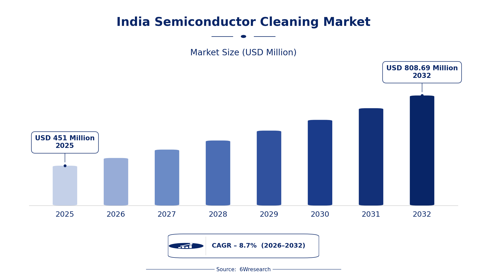
According to 6Wresearch internal database and industry insights, the India Semiconductor Cleaning Market was valued at USD 451.0 million in 2025 and is projected to reach USD 808.69 million by 2032, growing at a CAGR of approximately 8.7% during 2026–2032.
India Semiconductor Cleaning Market Highlights
| Report Metric | Details |
| Report Name | India Semiconductor Cleaning Market |
| Market Size 2025 | USD 451.0 million |
| Market Size 2032 | USD 808.69 million |
| Absolute Growth 2025–2032 | USD 357.69 million |
| CAGR 2026–2032 | 8.7% |
| Peak Annual Growth | 10.2% in 2026 |
| Forecast Period | 2026–2032 |
| Historical Data | 2022–2025 |
| Base Year | 2025 |
| Leading Cleaning Type, 2025 | Wet Cleaning (41% share) |
| Leading Equipment Used, 2025 | Acid/Base Baths (49% share) |
| Leading Process Application, 2025 | Pre-Lithography (38% share) |
| Leading End User, 2025 | Wafer Fabs (51% share) |
| Fastest-Growing Cleaning Type | Plasma Cleaning (10.0% CAGR) |
| Fastest-Growing Equipment Used | Plasma Chambers (10.7% CAGR) |
| Fastest-Growing Process Application | Post-Etch Residue Removal (11.5% CAGR) |
| Fastest-Growing End User | IC Packaging Facilities (10.4% CAGR) |
| Growing Sector | Wafer Fabrication |
| Key End Users | Wafer Fabs, IC Packaging Facilities, MEMS Manufacturers, Foundries |
India Semiconductor Cleaning Market Year-wise Growth Rate and Key Drivers (2022–2032)
This graph illustrates the annual growth rates of the market from 2022 to 2032, highlighting a steady upward trajectory and projected market expansion over the forecast period.
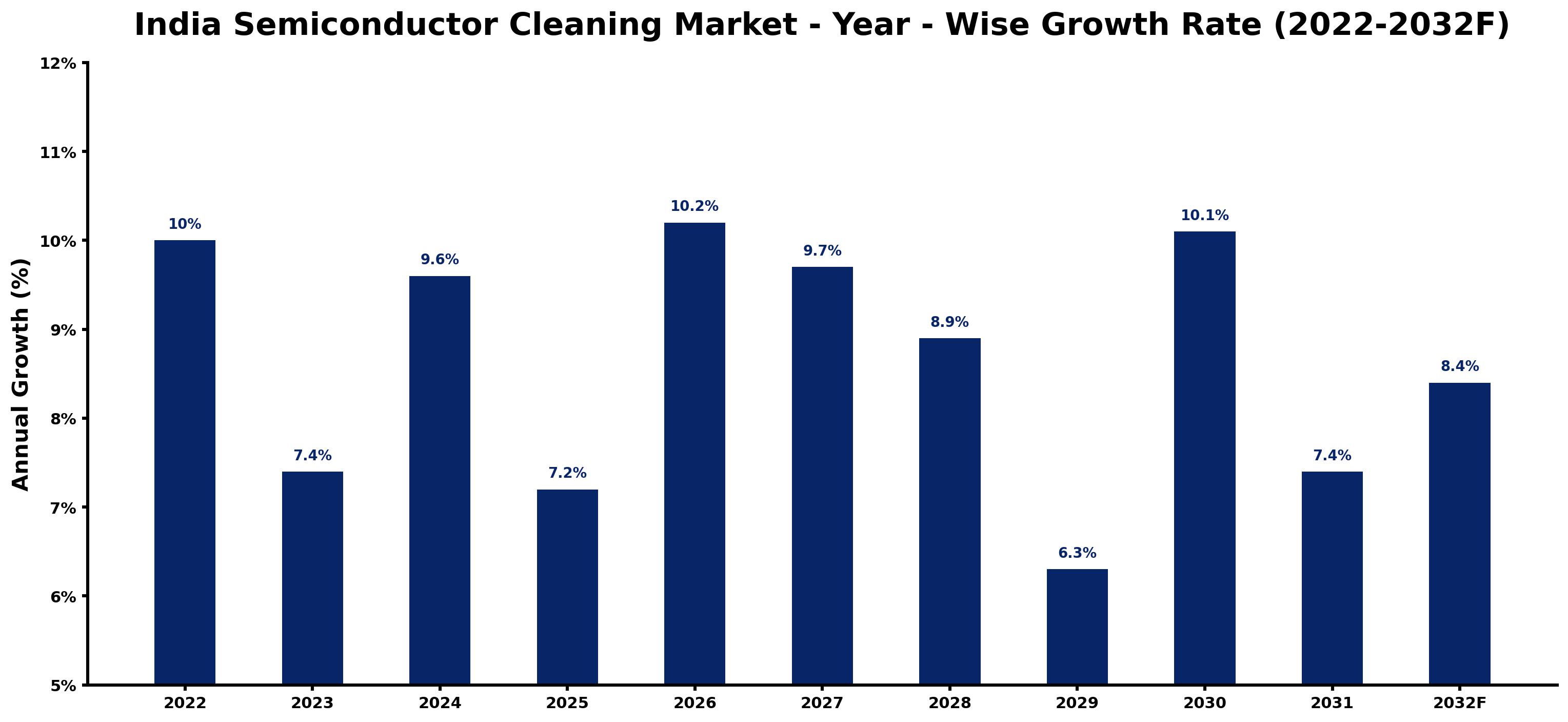
The following table presents the estimated annual growth rate for each year together with the principal factor influencing market performance.
| Year | Estimated Annual Growth (%) | Market Rationale |
| 2022 | 10.0 | The market experienced strong demand from domestic wafer fabs and foundries. |
| 2023 | 7.4 | Growth slowed due to initial adjustments in the semiconductor supply chain. |
| 2024 | 9.6 | Demand increased as manufacturers ramped up production capabilities. |
| 2025 | 7.2 | The market saw slower growth as investments stabilised in semiconductor technologies. |
| 2026 | 10.2 | Growth accelerated with the launch of the Semiconductor Mission attracting investments. |
| 2027 | 9.7 | A slight slowdown occurred as the market adjusted to new production capacities. |
| 2028 | 8.9 | Demand continued to slow as market conditions normalised after rapid growth. |
| 2029 | 6.3 | The market growth rate decreased as competition intensified among suppliers. |
| 2030 | 10.1 | Growth rebounded as new technologies and processes were adopted in fabs. |
| 2031 | 7.4 | The market saw a slowdown as the industry adjusted to evolving standards. |
| 2032 | 8.4 | Growth is projected to accelerate again with increased investments in semiconductor manufacturing. |
Note: Market size estimations and growth projections presented in this report are based on 6Wresearch's proprietary forecasting methodology, utilizing the latest available industry data, government publications, and primary research inputs.
India Semiconductor Cleaning Market Synopsis
Semiconductor Cleaning in India involves the removal of contaminants from semiconductor surfaces using chemical processes and specialized equipment. This process is crucial for preparing surfaces for lithography, etching, and bonding in semiconductor manufacturing. The India Semiconductor Cleaning Market is expanding due to rising demand from wafer fabs and foundries, supported by initiatives like the Semiconductor Mission. This initiative aims to improve local manufacturing capabilities and attract foreign investments, driving further growth in the sector.
Market Dynamics Impact Analysis (2026–2032)
| Factor | Type | Impact | Primary Segment Affected |
| Rising domestic demand from over 20 operational wafer fabs. | Driver | High | Wafer Fabs |
| Increased investments in semiconductor manufacturing technologies. | Driver | High | Foundries & OSATs |
| Investment opportunities in semiconductor cleaning equipment. | Opportunity | High | Plasma Chambers |
| Growing need for advanced cleaning processes in IC packaging. | Opportunity | High | IC Packaging Facilities |
| High costs associated with advanced cleaning technologies. | Restraint | High | Wet Cleaning |
| Limited availability of skilled workforce in semiconductor cleaning. | Restraint | Medium | Plasma Cleaning |
| The Semiconductor Cleaning Market faces challenges from high operational costs. | Challenge | High | Vapor Cleaning |
| Competition from international suppliers may hinder local growth. | Challenge | Medium | Cryogenic Cleaning |
Evaluation of Drivers in India Semiconductor Cleaning Market (2026–2032)
The factors lifting demand, and the evidence behind each, are summarised below.
| Drivers | Primary Segment Affected | Why It Matters (Evidence) |
| Increased production capacity at wafer fabs drives demand for cleaning processes. | Wafer Fabs | The installed base of semiconductor manufacturing equipment in India is estimated at $5 billion. |
| Growing investments in semiconductor technologies boost cleaning requirements. | Foundries & OSATs | The National Policy on Electronics aims to achieve $400 billion in electronics manufacturing by 2025. |
| The Semiconductor Mission attracts substantial investments for local manufacturing. | Plasma Chambers | The mission aims to attract $10 billion in investments for semiconductor manufacturing. |
| Demand for high-quality cleaning processes in IC packaging is rising. | IC Packaging Facilities | The Electronics and Semiconductor Manufacturing Cluster in Tamil Nadu aims to attract investments. |
| The need for advanced cleaning solutions increases with technology adoption. | Wet Cleaning | The Electronics Sector Skill Council of India promotes skill development in semiconductor technologies. |
Market growth for Semiconductor Cleaning in India is underpinned by increased production capacity at wafer fabs, growing investments in semiconductor technologies, and the Semiconductor Mission attracting substantial investments. The installed base of semiconductor manufacturing equipment in India is estimated at $5 billion, which drives demand for cleaning processes. Demand for high-quality cleaning processes in IC packaging is rising, with the Electronics and Semiconductor Manufacturing Cluster in Tamil Nadu aiming to attract investments. These factors contribute to a vibrant market for semiconductor cleaning solutions.
Evaluation of Restraints in India Semiconductor Cleaning Market
The key brakes on demand, and where they bite hardest, are shown below.
| Market Restraint | Primary Segment Affected | Why It Matters (Evidence) |
| High costs associated with advanced cleaning technologies limit market growth. | Wet Cleaning | The installed base of semiconductor manufacturing equipment is estimated at $5 billion, leading to high operational costs. |
| Limited availability of skilled workforce hampers operational efficiency. | Plasma Cleaning | The Electronics Sector Skill Council of India aims to improve skill development but faces challenges. |
| Competition from international suppliers affects local pricing strategies. | Vapor Cleaning | Local suppliers struggle to compete with established international players. |
| Regulatory compliance costs can be burdensome for manufacturers. | Cryogenic Cleaning | Compliance with Bureau of Indian Standards increases operational expenses. |
| Market fluctuations can impact investment in cleaning technologies. | Acid/Base Baths | Economic conditions influence funding for semiconductor manufacturing. |
India Semiconductor Cleaning Market Challenges
The India Semiconductor Cleaning Market faces high compliance costs due to stringent regulations from the Bureau of Indian Standards, which can delay product launches by up to six months for producers. Supply chain disruptions arise from reliance on imported cleaning chemicals, costing buyers approximately 20% of their production time during shortages. Buyers also deal with inefficiencies from outdated cleaning technologies, inflating operational costs by around 15%, which negatively impacts profitability. Furthermore, the shortage of skilled workers in semiconductor cleaning processes restricts suppliers' capacity to innovate, hindering the overall competitiveness of the market.
Trends in the India Semiconductor Cleaning Market
Below mentioned are some of the trends shaping the India Semiconductor Cleaning Market growth.
- Shift Towards Advanced Cleaning Techniques: Karnataka is experiencing a shift towards advanced cleaning techniques in semiconductor manufacturing, driven by the need for higher quality standards. The state is home to over 20 wafer fabs, which are increasingly adopting new technologies.
- Emergence of Plasma Cleaning: The Semiconductor Mission has led to the emergence of Plasma Cleaning technologies in India, which are gaining traction for their effectiveness. This segment is projected to grow at a CAGR of 10.0% from 2026 to 2032.
- Increase in Investment in IC Packaging: Investment in IC Packaging Facilities is on the rise, reflecting the growing demand for advanced semiconductor products. The sector is expected to grow at a CAGR of 10.4% as manufacturers seek to improve production capabilities.
- Growth in Post-Etch Residue Removal: Post-Etch Residue Removal has become a priority for semiconductor manufacturers, with a CAGR of 11.5% anticipated from 2026 to 2032. This trend highlights the increasing focus on quality in semiconductor processes.
Investment Opportunities in the India Semiconductor Cleaning Market
The following opportunities in the India Semiconductor Cleaning Market pair current demand with a clear way in.
- Supply of Advanced Cleaning Equipment: There is a growing opportunity to supply advanced cleaning equipment to semiconductor manufacturers, particularly in Karnataka, which has over 20 wafer fabs. The market is projected to grow as demand for quality increases.
- Investment in Semiconductor Cleaning Solutions: Now is an opportune time to invest in semiconductor cleaning solutions, driven by the Semiconductor Mission's goal of attracting $10 billion in investments. This initiative opens avenues for local partnerships and collaborations.
- Partnerships for Skill Development: Establishing partnerships for skill development in semiconductor cleaning can yield significant returns. The Electronics Sector Skill Council of India is actively promoting training programs to improve workforce capabilities.
- Expansion in Tamil Nadu's Semiconductor Cluster: Investing in the Electronics and Semiconductor Manufacturing Cluster in Tamil Nadu presents a unique opportunity. The cluster aims to attract investments, providing a conducive environment for new entrants.
Government Initiatives in the India Semiconductor Cleaning Market
The Ministry of Electronics and Information Technology announced a $1 billion incentive scheme in 2022 to promote semiconductor manufacturing in India. This scheme is designed to support various aspects of semiconductor production, including cleaning processes. The initiative aims to improve the competitiveness of local manufacturers and attract foreign investment. Furthermore, the Electronics Sector Skill Council of India is actively involved in funding skill development programs to ensure a skilled workforce for the semiconductor industry. These efforts are essential in meeting the increasing demand for skilled professionals in semiconductor cleaning.
The 'Semiconductor Mission' launched by the Ministry of Electronics and Information Technology in 2021 aims to attract $10 billion in investments for semiconductor manufacturing. This mission supports the development of infrastructure and capabilities necessary for local production, ensuring that manufacturers can meet the growing market demands effectively.
Future Insight of the India Semiconductor Cleaning Market
The India Semiconductor Cleaning Market will undergo substantial changes by 2032, driven by the Semiconductor Mission and the National Policy on Electronics. These initiatives will enhance local production capabilities and reduce reliance on imports. The installed base of semiconductor manufacturing equipment is projected to reach $7 billion, indicating a significant increase in investment. The Electronics and Semiconductor Manufacturing Cluster in Tamil Nadu will further promote advancements in cleaning techniques, leading to improved efficiency and productivity in semiconductor production.
Market Segmentation Analysis
Each segment group is reviewed below, with the leader by share and the fastest grower by CAGR.
By Cleaning Type – Wet Cleaning Dominated, Plasma Cleaning Expected to Grow Fastest
According to Shubham Padhi, Research Analyst at 6Wresearch, Wet Cleaning held a 41% share of the India Semiconductor Cleaning Market by cleaning type in 2025. Wet cleaning commands the largest share in the Indian Semiconductor Cleaning Market because it is essential for removing particles and contaminants from wafers. Its widespread application in over 20 operational wafer fabs across the country underscores its importance in semiconductor production. Over 2026–2032, Plasma Cleaning is expected to post the fastest growth, at a CAGR of 10.0%. Plasma cleaning is experiencing rapid growth due to its effectiveness in surface activation and cleaning prior to critical processes. The increasing complexity of semiconductor devices necessitates advanced cleaning techniques, ensuring plasma cleaning's continued adoption. Suppliers should focus on enhancing plasma cleaning technologies to meet the growing demands of the semiconductor sector.
By Equipment Used – Acid/Base Baths Dominated, Plasma Chambers Expected to Grow Fastest
With a 49% revenue share in 2025, Acid/Base Baths was the largest equipment used category. Acid/base baths hold the largest market share as they are vital for the effective cleaning of semiconductor surfaces. Their extensive use within the installed base of semiconductor manufacturing equipment, estimated at $5 billion, highlights their critical role in the industry. Plasma Chambers are projected to grow fastest, at a CAGR of 10.7% during 2026–2032. Plasma chambers are rapidly gaining traction because they play an integral role in plasma cleaning processes, essential for modern semiconductor manufacturing. The push for higher efficiency and quality in cleaning processes is propelling this growth. Buyers should consider investing in plasma chamber technology to remain competitive in the semiconductor market.
By Process Application – Pre-Lithography Dominated, Post-Etch Residue Removal Expected to Grow Fastest
The largest process application category in 2025 was Pre-Lithography, with a 38% share of total revenue. Pre-lithography cleaning leads the market share as it is crucial for preparing wafers before lithography, ensuring high-quality semiconductor production. This step is a key focus for wafer fabs, highlighting its importance in the manufacturing process. The quickest growth will come from Post-Etch Residue Removal, forecast to expand at a CAGR of 11.5% between 2026 and 2032. Post-etch residue removal is the fastest-growing application, driven by the need to maintain quality in etching processes during semiconductor fabrication. As the demand for precision in semiconductor devices increases, this process becomes increasingly essential. Suppliers must improve their capabilities in post-etch residue removal to meet the rising standards in semiconductor manufacturing.
By End User – Wafer Fabs Dominated, IC Packaging Facilities Expected to Grow Fastest
In 2025, Wafer Fabs led the end user split with a 51% share. Wafer fabs command the largest share of the market as they are the primary users of cleaning processes in semiconductor production. Their substantial investment in cleaning technologies underscores their central role in the semiconductor supply chain. IC Packaging Facilities are set to record the highest CAGR in this split, 10.4% over 2026–2032. IC packaging facilities are the fastest-growing end user segment, as they increasingly require cleaning processes for effective packaging. The expansion of the semiconductor market drives the need for advanced cleaning solutions in this sector. Suppliers should focus on targeting IC packaging facilities to capitalise on the growth opportunities in the semiconductor cleaning market.
Key Attractiveness of the Report
- 10 Years of Market Numbers
- Historical Data Starting from 2022 to 2025
- Base Year 2025
- Forecast Data until 2032
- Key Performance Indicators Impacting the Market
- Major Upcoming Developments and Projects
Key Highlights of the Report:
- India Semiconductor Cleaning Market Outlook
- Market Size of India Semiconductor Cleaning Market, 2025
- Forecast of India Semiconductor Cleaning Market, 2032
- Historical Data and Forecast of India Semiconductor Cleaning Revenues & Volume for the Period 2022 - 2032F
- India Semiconductor Cleaning Market Trend Evolution
- India Semiconductor Cleaning Market Drivers and Challenges
- India Semiconductor Cleaning Price Trends
- India Semiconductor Cleaning Porter's Five Forces
- India Semiconductor Cleaning Industry Life Cycle
- Historical Data and Forecast of India Semiconductor Cleaning Market Revenues & Volume By Cleaning Type for the Period 2022 - 2032F
- Historical Data and Forecast of India Semiconductor Cleaning Market Revenues & Volume By Wet Cleaning for the Period 2022 - 2032F
- Historical Data and Forecast of India Semiconductor Cleaning Market Revenues & Volume By Plasma Cleaning for the Period 2022 - 2032F
- Historical Data and Forecast of India Semiconductor Cleaning Market Revenues & Volume By Vapor Cleaning for the Period 2022 - 2032F
- Historical Data and Forecast of India Semiconductor Cleaning Market Revenues & Volume By Cryogenic Cleaning for the Period 2022 - 2032F
- Historical Data and Forecast of India Semiconductor Cleaning Market Revenues & Volume By Equipment Used for the Period 2022 - 2032F
- Historical Data and Forecast of India Semiconductor Cleaning Market Revenues & Volume By Acid/Base Baths for the Period 2022 - 2032F
- Historical Data and Forecast of India Semiconductor Cleaning Market Revenues & Volume By Plasma Chambers for the Period 2022 - 2032F
- Historical Data and Forecast of India Semiconductor Cleaning Market Revenues & Volume By Solvent-Based Systems for the Period 2022 - 2032F
- Historical Data and Forecast of India Semiconductor Cleaning Market Revenues & Volume By CO Ice Blast for the Period 2022 - 2032F
- Historical Data and Forecast of India Semiconductor Cleaning Market Revenues & Volume By Process Application for the Period 2022 - 2032F
- Historical Data and Forecast of India Semiconductor Cleaning Market Revenues & Volume By Pre-Lithography for the Period 2022 - 2032F
- Historical Data and Forecast of India Semiconductor Cleaning Market Revenues & Volume By Post-Etch Residue Removal for the Period 2022 - 2032F
- Historical Data and Forecast of India Semiconductor Cleaning Market Revenues & Volume By Substrate Pre-Bonding for the Period 2022 - 2032F
- Historical Data and Forecast of India Semiconductor Cleaning Market Revenues & Volume By Sensitive Surface Cleaning for the Period 2022 - 2032F
- Historical Data and Forecast of India Semiconductor Cleaning Market Revenues & Volume By End User for the Period 2022 - 2032F
- Historical Data and Forecast of India Semiconductor Cleaning Market Revenues & Volume By Wafer Fabs for the Period 2022 - 2032F
- Historical Data and Forecast of India Semiconductor Cleaning Market Revenues & Volume By IC Packaging Facilities for the Period 2022 - 2032F
- Historical Data and Forecast of India Semiconductor Cleaning Market Revenues & Volume By MEMS Manufacturers for the Period 2022 - 2032F
- Historical Data and Forecast of India Semiconductor Cleaning Market Revenues & Volume By Foundries & OSATs for the Period 2022 - 2032F
- India Semiconductor Cleaning Import Export Trade Statistics
- Market Opportunity Assessment By Cleaning Type
- Market Opportunity Assessment By Equipment Used
- Market Opportunity Assessment By Process Application
- Market Opportunity Assessment By End User
- India Semiconductor Cleaning Top Companies Market Share
- India Semiconductor Cleaning Competitive Benchmarking By Technical and Operational Parameters
- India Semiconductor Cleaning Company Profiles
- India Semiconductor Cleaning Key Strategic Recommendations
Market Covered
Segments analysed in this report are listed below.
By Cleaning Type
- Wet Cleaning
- Plasma Cleaning
- Vapor Cleaning
- Cryogenic Cleaning
By Equipment Used
- Acid/Base Baths
- Plasma Chambers
- Solvent-Based Systems
- CO₂ Ice Blast
By Process Application
- Pre-Lithography
- Post-Etch Residue Removal
- Substrate Pre-Bonding
- Sensitive Surface Cleaning
By End User
- Wafer Fabs
- IC Packaging Facilities
- MEMS Manufacturers
- Foundries & OSATs