Japan Advanced Semiconductor Packaging Market Size & Growth Rate
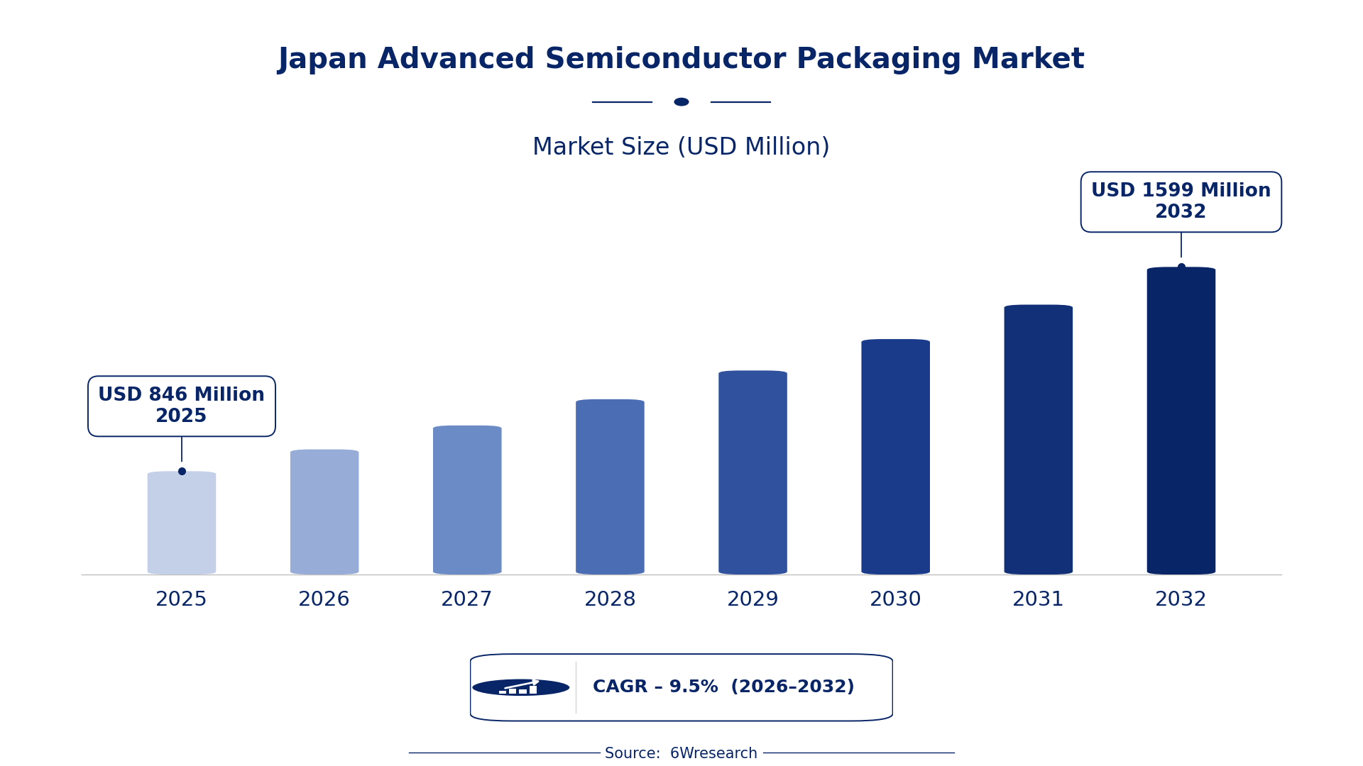
According to 6Wresearch internal database and industry insights, the Japan Advanced Semiconductor Packaging Market was valued at USD 846 Million in 2025 and is projected to reach USD 1,599 Million by 2032, growing at a CAGR of approximately 9.5% during 2026–2032.
Japan Advanced Semiconductor Packaging Market Highlights
| Report Metric | Details |
| Report Name | Japan Advanced Semiconductor Packaging Market (2026-2032) |
| Market Size 2025 | USD 846 Million |
| Market Size 2032 | USD 1,599 Million |
| Absolute Growth 2025–2032 | USD 753 Million |
| CAGR 2026–2032 | 9.5% |
| Peak Annual Growth | 14.3% in 2032 |
| Forecast Period | 2026–2032 |
| Historical Data | 2022–2025 |
| Base Year | 2025 |
| Leading Packaging Type, 2025 | Fan-out Wafer-Level Packaging (45% share) |
| Fastest-Growing Packaging Type | Fan-in Wafer-Level Packaging (14.3% CAGR) |
| Growing Sector | Consumer Electronics |
| Key End Users | Automotive manufacturers, consumer electronics producers, industrial equipment manufacturers |
Japan Advanced Semiconductor Packaging Market Year-wise Growth Rate and Key Drivers (2022–2032)
This graph illustrates the annual growth rates of the market from 2022 to 2032, highlighting a steady upward trajectory and projected market expansion over the forecast period.
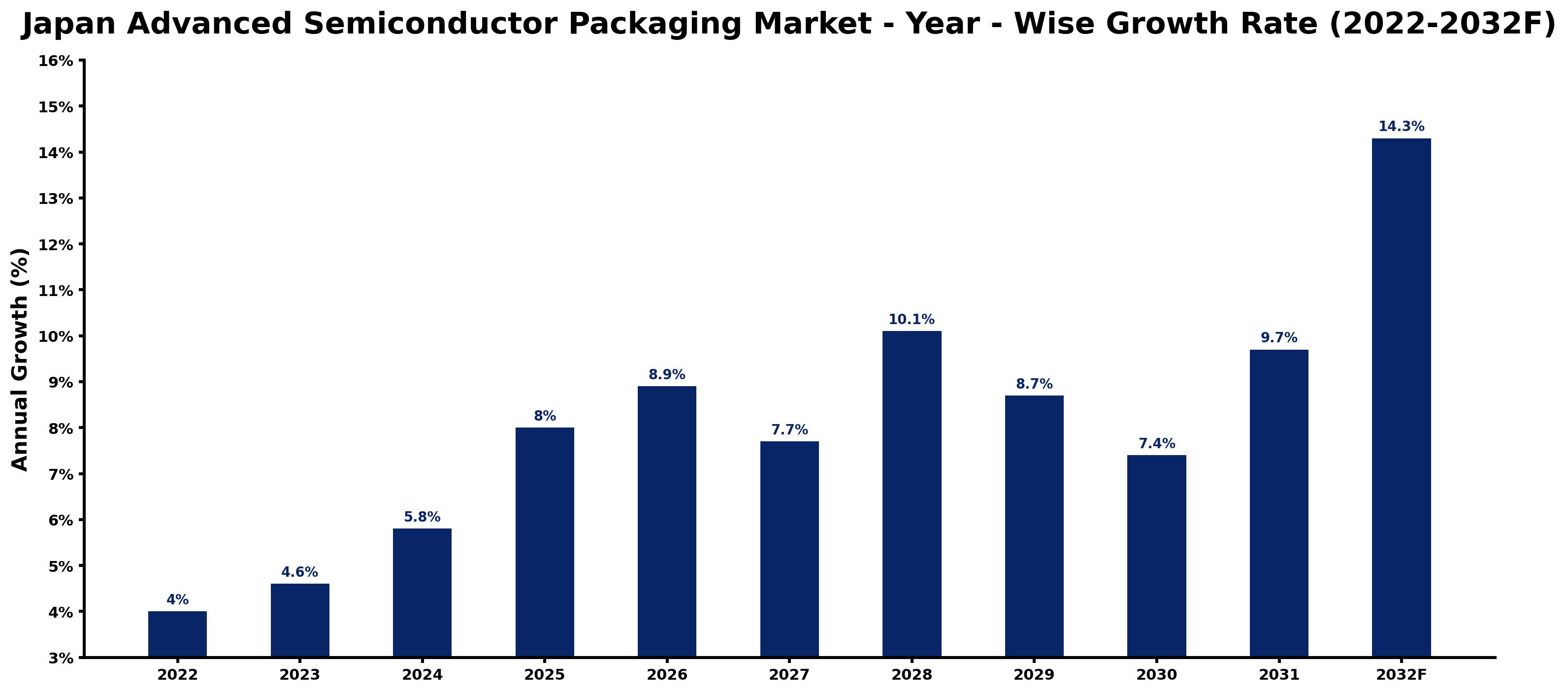
Below, each year's estimated growth is shown next to the factor that most influenced it.
| Year | Estimated Annual Growth (%) | Market Rationale |
| 2022 | 4.0 | The market showed steady activity, reflecting ongoing demand from consumer electronics. |
| 2023 | 4.6 | Growth accelerated as consumer electronics and automotive sectors increased their investments. |
| 2024 | 5.8 | The rise in smartphone production further boosted demand for advanced packaging solutions. |
| 2025 | 8.0 | The market peaked as automotive and industrial applications expanded significantly. |
| 2026 | 8.9 | Growth continued as technology advancements drove higher efficiency requirements in packaging. |
| 2027 | 7.7 | Growth slowed slightly due to market saturation in certain consumer electronics segments. |
| 2028 | 10.1 | Demand surged again with increased adoption of advanced packaging in electric vehicles. |
| 2029 | 8.7 | A slight slowdown occurred as the market adjusted to new production capacities. |
| 2030 | 7.4 | Growth moderated as companies focused on optimising existing packaging technologies. |
| 2031 | 9.7 | The market rebounded with renewed investments in semiconductor R&D and innovation. |
| 2032 | 14.3 | Growth peaked as advanced packaging became essential for high-performance computing. |
Note: Market size estimations and growth projections presented in this report are based on 6Wresearch's proprietary forecasting methodology, utilizing the latest available industry data, government publications, and primary research inputs.
Japan Advanced Semiconductor Packaging Market Synopsis
Advanced Semiconductor Packaging encapsulates and connects semiconductor devices, utilising wafer fabrication, die bonding, and encapsulation techniques. This technology improves performance, reduces size, and enhances thermal management for electronic devices. The Japan Advanced Semiconductor Packaging Market is expanding, driven by domestic demand from consumer electronics, automotive, and industrial applications. With over 10 million semiconductor units produced in 2023, investment in semiconductor R&D reached 100 billion yen, underscoring the increasing focus on innovation and efficiency in packaging technologies.
Market Dynamics Impact Analysis (2026–2032)
| Factor | Type | Impact | Primary Segment Affected |
| Growing demand for compact and efficient electronic devices | Driver | High | Fan-in Wafer-Level Packaging |
| Increased adoption of advanced packaging in electric vehicles | Driver | High | Fan-out Wafer-Level Packaging |
| Expansion of semiconductor manufacturing capabilities in the Tokyo region | Opportunity | High | Flip Chip |
| Rising consumer demand for high-performance electronics | Opportunity | Medium | Fan-in Wafer-Level Packaging |
| High costs associated with advanced packaging technologies | Restraint | High | Flip Chip |
| Limited availability of skilled workforce in semiconductor packaging | Restraint | Medium | Fan-out Wafer-Level Packaging |
| Compliance with evolving industry standards and regulations | Challenge | High | 2.5/3D |
| Capacity constraints in semiconductor manufacturing facilities | Challenge | Medium | Fan-in Wafer-Level Packaging |
Evaluation of Drivers in Japan Advanced Semiconductor Packaging Market (2026–2032)
These are the developments adding the most demand over the forecast period.
| Drivers | Primary Segment Affected | Why It Matters (Evidence) |
| Increased smartphone production | Fan-out Wafer-Level Packaging | Over 10 million units produced in 2023, driving demand for advanced packaging solutions. |
| Growing automotive sector | Fan-in Wafer-Level Packaging | The Automotive Industry Association promotes advanced packaging for electric vehicles, contributing to rising demand with a projected increase of 30%. |
| Rising consumer electronics demand | Flip Chip | Fan-in Wafer-Level Packaging is used in over 60% of consumer electronics, boosting production needs significantly. |
| Investment in semiconductor R&D | 2.5/3D | Investment reached 100 billion yen in 2023, driving innovation in packaging technologies. |
| Technological advancements in packaging | Fan-out Wafer-Level Packaging | The JIS Z 8701 standard governs packaging, ensuring quality and performance in production. |
Purchasing is picking up as the automotive sector increasingly adopts advanced packaging for electric vehicles, driving higher production needs. In 2023, over 10 million semiconductor units were produced using advanced packaging, reflecting the rising interest from consumer electronics. The Tokyo region remains a major hub for semiconductor manufacturing, further boosting the need for innovative packaging solutions. Investment in semiconductor R&D reached 100 billion yen, driving technological advancements and efficiency improvements. The growing adoption of advanced packaging technologies is evident in the increasing use of Flip Chip solutions in high-performance applications.
Evaluation of Restraints in Japan Advanced Semiconductor Packaging Market
Several factors work against faster growth; the main ones are summarised below.
| Market Restraint | Primary Segment Affected | Why It Matters (Evidence) |
| High costs of advanced packaging technologies | Flip Chip | The complexity of manufacturing processes increases costs, affecting market accessibility by up to 20%. |
| Limited availability of skilled workforce | Fan-out Wafer-Level Packaging | A shortage of trained professionals hampers production efficiency and innovation, affecting output by up to 15%. |
| Compliance with industry standards | 2.5/3D | Evolving regulations require constant updates to manufacturing processes, adding operational burdens and costs. |
| Market saturation in consumer electronics | Fan-in Wafer-Level Packaging | High competition and established products limit growth opportunities in this segment. |
| Dependency on semiconductor supply chain stability | Fan-out Wafer-Level Packaging | Disruptions in the supply chain can delay production and increase costs. |
Japan Advanced Semiconductor Packaging Market Challenges
Producers face rising costs due to outdated manufacturing technologies, increasing production expenses by 15% and squeezing profit margins. Importers encounter challenges with limited access to advanced packaging materials, which can delay supply chains and extend lead times by three weeks. Buyers struggle with skills shortages as the workforce lacks expertise in modern packaging techniques, potentially reducing production efficiency by 20%. Regulatory compliance with the JIS Z 8701 standard complicates operations, leading to increased costs for manufacturers, estimated at 5% of total expenses.
Trends in the Japan Advanced Semiconductor Packaging Market
Below are the shifts with the largest effect on the Japan Advanced Semiconductor Packaging Market.
- Shift from Traditional to Advanced Packaging Techniques: The Tokyo region is experiencing a shift towards advanced packaging techniques, with Fan-out Wafer-Level Packaging increasingly adopted in smartphones and tablets, reflecting a rise in usage since 2020.
- Transition from 2D to 3D Packaging: In 2023, the trend towards 3D packaging technologies began gaining traction, supported by the Tokyo University of Science's research, aiming to improve performance in high-density applications.
- Emergence of Electric Vehicles Driving Packaging Innovation: The automotive sector is prioritising advanced packaging solutions, with the Automotive Industry Association reporting a notable increase in demand for Fan-in Wafer-Level Packaging for electric vehicles.
- Rising Focus on Sustainability in Packaging: The Plastic Resource Circulation Act is promoting sustainable practices in semiconductor packaging, with an increase in biodegradable materials being used since its implementation.
Investment Opportunities in the Japan Advanced Semiconductor Packaging Market
The openings below show where demand in the Japan Advanced Semiconductor Packaging Market is visible and how suppliers can enter.
- Gap in High-Performance Packaging Solutions: With a projected increase in demand for high-performance electronics, suppliers can focus on Fan-out Wafer-Level Packaging to meet this need in the Tokyo region, where production is expected to rise by 25%.
- Growing Demand from Automotive Sector: The automotive industry is increasingly adopting advanced packaging, creating opportunities for suppliers to provide Flip Chip solutions in electric vehicles, with demand expected to grow by 30%.
- Need for Sustainable Packaging Solutions: With the Plastic Resource Circulation Act promoting eco-friendly practices, there is an opportunity to develop biodegradable packaging materials for semiconductor applications, targeting a market share increase of 15%.
- Investment in Semiconductor R&D: Investment in semiconductor R&D reached 100 billion yen in 2023, providing a chance for collaboration with research institutions to innovate packaging technologies.
Government Initiatives in the Japan Advanced Semiconductor Packaging Market
The Food Sanitation Act amendment, fully applied in June 2021, mandates HACCP-based hygiene management for food businesses, indirectly affecting semiconductor packaging standards. The Plastic Resource Circulation Act, enacted in 2021, promotes the reduction, reuse, and recycling of plastics, encouraging semiconductor producers to adopt sustainable practices in packaging.
The Japan Electronics and Information Technology Industries Association (JEITA) oversees funding for semiconductor technology advancements, approving projects that improve packaging efficiency and innovation. The Ministry of Economy, Trade and Industry (METI) also plays a role in setting industry standards, ensuring compliance among producers.
Future Insight of the Japan Advanced Semiconductor Packaging Market
New semiconductor research facilities will emerge by 2032, driven by government initiatives and a focus on advanced technologies. Automation technologies will streamline production processes, allowing suppliers to reduce lead times by up to 30%. Improved packaging standards will enhance product reliability, benefiting buyers in consumer electronics. Collaborations between academic institutions and industry will drive innovation, ensuring Japan maintains its leadership in semiconductor technology advancements.
Market Segmentation Analysis
Japan Advanced Semiconductor Packaging Market report covers a detailed analysis of the following market segments:
By Packaging Type – Fan-out Wafer-Level Packaging Leads, Fan-in Wafer-Level Packaging Expected to Grow Fastest
According to Sumit Sagar, AM at 6Wresearch, Fan-out Wafer-Level Packaging held 45% of the Japan Advanced Semiconductor Packaging Market by packaging type in 2025. Fan-out Wafer-Level Packaging dominates the market due to its prevalent application in high-density consumer electronics, particularly smartphones and tablets. The strong semiconductor manufacturing ecosystem in the Tokyo region supports a robust supply chain for this advanced packaging technology. Fan-in Wafer-Level Packaging is projected to grow fastest, at a CAGR of 14.3% during 2026–2032. Fan-in Wafer-Level Packaging is experiencing rapid growth driven by the demand for compact devices, with over 60% of consumer electronics utilising this packaging method. The emphasis on efficient space management in electronic devices is a crucial factor behind this segment's acceleration. Suppliers should focus on developing solutions for Fan-in Wafer-Level Packaging to meet the growing needs of compact device manufacturers.
Key Attractiveness of the Report
- 10 Years of Market Numbers
- Historical Data Starting from 2022 to 2025
- Base Year 2025
- Forecast Data until 2032
- Key Performance Indicators Impacting the Market
- Major Upcoming Developments and Projects
Key Highlights of the Report:
- Japan Advanced Semiconductor Packaging Market Outlook
- Market Size of Japan Advanced Semiconductor Packaging Market, 2025
- Forecast of Japan Advanced Semiconductor Packaging Market, 2032
- Historical Data and Forecast of Japan Advanced Semiconductor Packaging Revenues & Volume for the Period 2022-2032
- Japan Advanced Semiconductor Packaging Market Trend Evolution
- Japan Advanced Semiconductor Packaging Market Drivers and Challenges
- Japan Advanced Semiconductor Packaging Price Trends
- Japan Advanced Semiconductor Packaging Porter's Five Forces
- Japan Advanced Semiconductor Packaging Industry Life Cycle
- Historical Data and Forecast of Japan Advanced Semiconductor Packaging Market Revenues & Volume By Packaging Type for the Period 2022-2032
- Historical Data and Forecast of Japan Advanced Semiconductor Packaging Market Revenues & Volume By Fan-out Wafer-Level Packaging for the Period 2022-2032
- Historical Data and Forecast of Japan Advanced Semiconductor Packaging Market Revenues & Volume By Fan-in Wafer-Level Packaging for the Period 2022-2032
- Historical Data and Forecast of Japan Advanced Semiconductor Packaging Market Revenues & Volume By Flip Chip for the Period 2022-2032
- Historical Data and Forecast of Japan Advanced Semiconductor Packaging Market Revenues & Volume By 2.5/3D for the Period 2022-2032
- Japan Advanced Semiconductor Packaging Import Export Trade Statistics
- Market Opportunity Assessment By Packaging Type
- Japan Advanced Semiconductor Packaging Top Companies Market Share
- Japan Advanced Semiconductor Packaging Competitive Benchmarking By Technical and Operational Parameters
- Japan Advanced Semiconductor Packaging Company Profiles
- Japan Advanced Semiconductor Packaging Key Strategic Recommendations
Market Covered
This report examines the market across the segments below.
By Packaging Type
- Fan-out Wafer-Level Packaging
- Fan-in Wafer-Level Packaging
- Flip Chip
- 2.5/3D