Japan Arsenic Sulfide Sputtering Target Market Size & Growth Rate
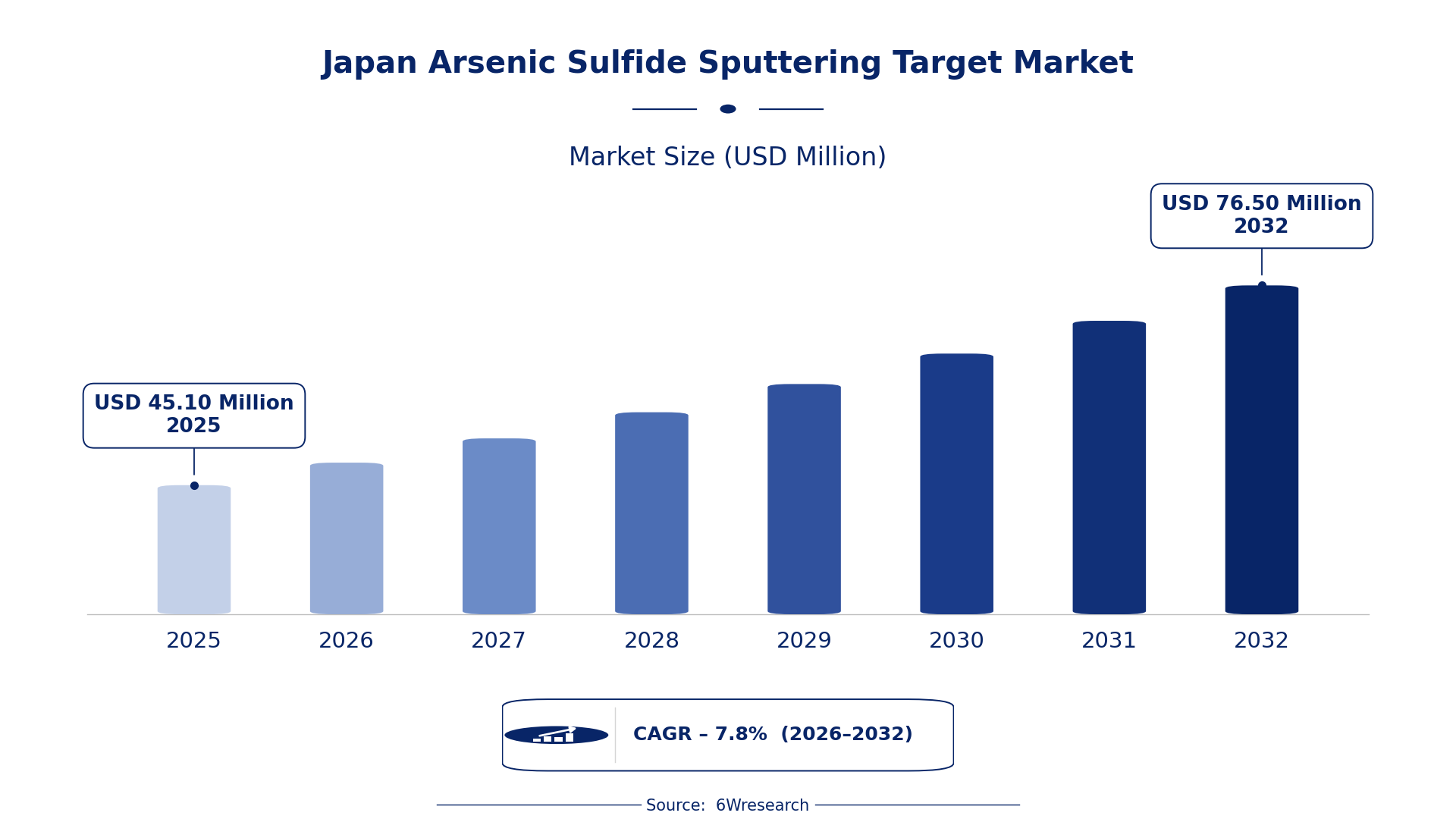
According to 6Wresearch internal database and industry insights, the Japan Arsenic Sulfide Sputtering Target Market was valued at USD 45.10 Million in 2025 and is projected to reach USD 76.50 Million by 2032, growing at a CAGR of approximately 7.8% during 2026–2032.
Japan Arsenic Sulfide Sputtering Target Market Highlights
| Report Metric | Details |
| Report Name | Japan Arsenic Sulfide Sputtering Target Market (2026-2032) |
| Market Size 2025 | USD 45.10 Million |
| Market Size 2032 | USD 76.50 Million |
| Absolute Growth 2025–2032 | USD 31.40 Million |
| CAGR 2026–2032 | 7.8% |
| Peak Annual Growth | 8.5% in 2026 |
| Forecast Period | 2026–2032 |
| Historical Data | 2022–2025 |
| Base Year | 2025 |
| Leading Product Type, 2025 | Purity 99.999% (40% share) |
| Leading Application, 2025 | Semiconductor (41% share) |
| Fastest-Growing Application | Chemical Vapor Deposition (10.4% CAGR) |
| Growing Sector | Chemical Vapor Deposition |
| Key End Users | Semiconductor, Chemical Vapor Deposition, Physical Vapor Deposition |
Japan Arsenic Sulfide Sputtering Target Market Year-wise Growth Rate and Key Drivers (2022–2032)
This graph illustrates the annual growth rates of the market from 2022 to 2032, highlighting a steady upward trajectory and projected market expansion over the forecast period.
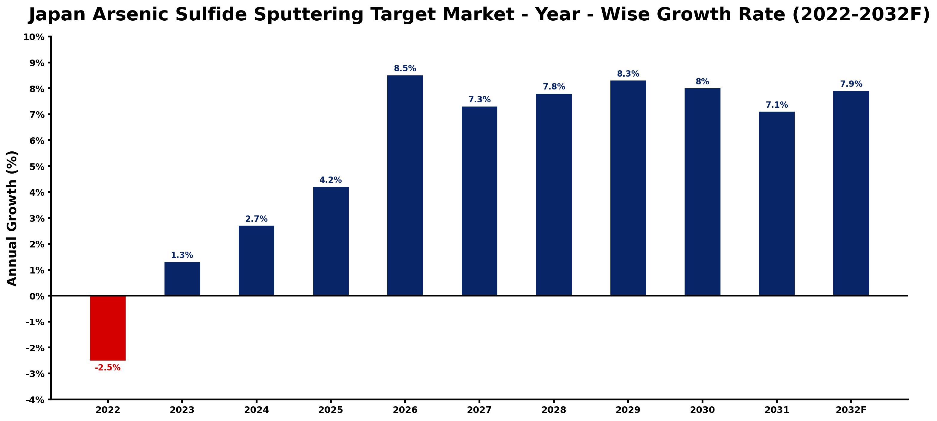
Annual growth estimates for each year appear below with the principal reason behind them, explaining the shifts that set the pace of the market.
| Year | Estimated Annual Growth (%) | Market Rationale |
| 2022 | -2.5 | The market faced challenges due to reduced semiconductor production activities. |
| 2023 | 1.3 | Growth returned as domestic manufacturers increased production levels. |
| 2024 | 2.7 | Demand continued to rise with advancements in semiconductor technologies. |
| 2025 | 4.2 | The market showed positive momentum driven by increased investments in semiconductor fabrication. |
| 2026 | 8.5 | A peak in growth is expected as new facilities come online and production expands. |
| 2027 | 7.3 | Growth is projected to slow slightly as the market adjusts to the rapid expansion of the previous year. |
| 2028 | 7.8 | Demand is expected to pick up again as technology upgrades in semiconductor processes are implemented. |
| 2029 | 8.3 | Growth is projected to continue as companies invest in advanced lithography techniques. |
| 2030 | 8.0 | The market is expected to experience a slowdown as production capacity stabilises after previous surges. |
| 2031 | 7.1 | Growth is projected to moderate as manufacturers focus on efficiency and optimisation. |
| 2032 | 7.9 | Demand is expected to rise again as new semiconductor projects are initiated. |
Note: Market size estimations and growth projections presented in this report are based on 6Wresearch's proprietary forecasting methodology, utilizing the latest available industry data, government publications, and primary research inputs.
Japan Arsenic Sulfide Sputtering Target Market Synopsis
Arsenic sulfide sputtering targets serve as critical materials in thin-film deposition processes, particularly for semiconductor applications. The Japan Arsenic Sulfide Sputtering Target Market is driven by a semiconductor sector valued at over ¥3 trillion, which fuels demand for high-purity sputtering targets, especially those with 99.999% purity. The recent ¥500 billion investment in semiconductor technology development and ongoing support from the Ministry of Economy, Trade and Industry are key factors behind this growth, ensuring a steady supply of advanced materials for domestic manufacturers.
Market Dynamics Impact Analysis (2026–2032)
| Factor | Type | Impact | Primary Segment Affected |
| Increased investment in semiconductor technology development | Driver | High | Semiconductor |
| Rising demand for high-purity materials in advanced applications | Driver | High | Purity 99.999% |
| Growing semiconductor manufacturing capacity in Tokyo and Osaka | Opportunity | High | Semiconductor |
| Expansion of Chemical Vapor Deposition techniques | Opportunity | Medium | Chemical Vapor Deposition |
| Regulatory compliance costs for chemical substances | Restraint | Medium | Purity 99.999% |
| Limited availability of high-purity arsenic sulfide | Restraint | High | Purity 99.999% |
| High production costs for advanced materials | Challenge | High | Purity 99.999% |
| Competition from alternative deposition materials | Challenge | Medium | Physical Vapor Deposition |
Evaluation of Drivers in Japan Arsenic Sulfide Sputtering Target Market (2026–2032)
The table below links each growth driver to the segment it affects and the evidence for it.
| Drivers | Primary Segment Affected | Why It Matters (Evidence) |
| Investment in semiconductor fabrication equipment | Semiconductor | Japan's installed base exceeds 1,200 units, driving demand for sputtering targets. |
| Technological advancements in semiconductor processes | Purity 99.999% | The shift towards advanced lithography requires high-purity materials. |
| Increased production of consumer electronics | Semiconductor | Japan's population of 125 million boosts demand for electronics. |
| Growth in Chemical Vapor Deposition applications | Chemical Vapor Deposition | This technique is widely used, increasing the need for sputtering targets. |
| Support from the Ministry of Economy, Trade and Industry | Semiconductor | Innovation programs stimulate demand for advanced materials. |
Most of the extra volume comes from increased investments in semiconductor fabrication equipment, with over 1,200 units installed in Japan. The semiconductor sector, valued at over ¥3 trillion, drives demand for high-purity arsenic sulfide sputtering targets. Technological advancements in semiconductor processes, particularly in advanced lithography, require materials with 99.999% purity. The growing production of consumer electronics, spurred by Japan's population of 125 million, further boosts demand.
Evaluation of Restraints in Japan Arsenic Sulfide Sputtering Target Market
The key brakes on demand, and where they bite hardest, are shown below.
| Market Restraint | Primary Segment Affected | Why It Matters (Evidence) |
| High costs associated with regulatory compliance for chemical substances | Purity 99.999% | Compliance with the PRTR Law increases operational expenses for manufacturers. |
| Limited supply of high-purity arsenic sulfide | Purity 99.999% | The scarcity of raw materials constrains production capabilities. |
| Fluctuating prices of raw materials | Purity 99.999% | Volatility in raw material costs affects pricing strategies for producers. |
| Technological limitations in production processes | Purity 99.9% | Current production methods may not meet rising purity demands. |
| Competition from alternative materials in deposition processes | Physical Vapor Deposition | Emerging materials may reduce reliance on arsenic sulfide targets. |
Japan Arsenic Sulfide Sputtering Target Market Challenges
Buyers encounter supply chain disruptions due to reliance on a limited number of domestic producers, which can delay the acquisition of arsenic sulfide sputtering targets by up to four weeks. Skills shortages affect suppliers since the semiconductor industry requires highly specialised knowledge, leading to training periods of six months that can stall production schedules. Technology gaps arise as some suppliers lack access to advanced purification processes, resulting in rejection rates for targets that can increase by 15%. Regulatory compliance with standards like JIS Z 2801 complicates operations, imposing additional costs on suppliers who must ensure their products meet these requirements before market entry.
Trends in the Japan Arsenic Sulfide Sputtering Target Market
Four trends stand out in the Japan Arsenic Sulfide Sputtering Target Market.
- Shift towards Advanced Lithography Techniques: In 2022, Japan's semiconductor manufacturers increasingly adopted advanced lithography techniques, requiring high-purity materials. Over 10,000 tons of arsenic sulfide were produced to meet this demand.
- Emergence of Chemical Vapor Deposition: The Chemical Vapor Deposition technique is gaining traction among semiconductor manufacturers in Japan, with a projected CAGR of 10.4% from 2026 to 2032, reflecting a shift in production methodologies.
- Growing Focus on Sustainability in Semiconductor Production: Manufacturers are prioritising sustainable practices, supported by the Economic Security Promotion Act. This law encourages investments in eco-friendly technologies and supply-chain resilience.
- Expansion of Semiconductor Manufacturing Hubs: Tokyo and Osaka are solidifying their positions as major semiconductor manufacturing hubs, with investments exceeding ¥500 billion in technology development, boosting local production capabilities.
Investment Opportunities in the Japan Arsenic Sulfide Sputtering Target Market
Several openings in the Japan Arsenic Sulfide Sputtering Target Market merit attention from investors.
- Timing for Investment: With a projected market size of USD 76.50 million by 2032, there is a strong opportunity for suppliers to invest in high-purity arsenic sulfide sputtering targets. Semiconductor manufacturers in Tokyo are actively seeking reliable sources.
- Demand from Semiconductor Manufacturers: The semiconductor sector, valued at over ¥3 trillion, presents a prime opportunity for suppliers of high-purity materials. Collaborating with local manufacturers can facilitate market entry.
- Entry through Joint Ventures: Establishing joint ventures with local semiconductor firms can ease access to the growing market. The demand for advanced materials is rising, driven by innovation.
- Gap in High-Purity Materials: The market gap for high-purity arsenic sulfide sputtering targets is clear, with increasing demand from advanced lithography processes. Suppliers can capitalise on this niche.
Government Initiatives in the Japan Arsenic Sulfide Sputtering Target Market
The Economic Security Promotion Act (2022) enhances the existing framework by ensuring supply-chain resilience for critical materials like arsenic sulfide sputtering targets. This law mandates that producers maintain a steady supply of these materials, which is vital for the semiconductor industry. It complements the PRTR Law and the Chemical Substances Control Law, which focus on environmental safety and chemical management, respectively, ensuring that production processes align with sustainability goals.
Buyers in the semiconductor sector benefit from the support provided by the Ministry of Economy, Trade and Industry's innovation programs. These initiatives fund research and development projects that enhance production capabilities. In 2023, the ministry allocated ¥500 billion to boost semiconductor technology, enabling manufacturers to access higher-quality arsenic sulfide sputtering targets and improve their production efficiency.
Future Insight of the Japan Arsenic Sulfide Sputtering Target Market
New advanced purification facilities will be operational by 2032, backed by government initiatives aimed at semiconductor innovation. The Ministry of Economy, Trade and Industry's programmes seek to elevate production capabilities. With ¥500 billion invested in 2023, advancements in purification technologies will improve target quality. Buyers will gain access to a more consistent supply of high-purity arsenic sulfide sputtering targets, while suppliers will benefit from streamlined processes that comply with international standards.
Market Segmentation Analysis
Japan Arsenic Sulfide Sputtering Target Market report covers a detailed analysis of the following market segments:
By Product Type – Purity 99.999% Leads and Records the Fastest Growth
According to Ravi Bhandari, Research Head at 6Wresearch, Purity 99.999% accounted for 40% of the market by product type in 2025. Purity 99.999% targets dominate the market as they are vital for advanced lithography processes in high-performance semiconductor manufacturing. Their necessity is underscored by the significant installed base of over 1,200 semiconductor fabrication units in Japan. The same category is also set to grow fastest, at a CAGR of 11.1% during 2026–2032. The growth of Purity 99.999% targets is propelled by Japan's ¥500 billion investment in semiconductor technology development, which aims to foster innovation in the industry. This investment will likely lead to an increased adoption of these high-purity materials, widening their market lead. Suppliers must scale up production of Purity 99.999% targets to meet the rising demand driven by technological advancements.
By Application – Semiconductor Leads, Chemical Vapor Deposition Expected to Grow Fastest
Semiconductor held 41% of the Japan Arsenic Sulfide Sputtering Target Market by application in 2025. The semiconductor application leads the market as it is the cornerstone of Japan's electronics manufacturing, valued at over ¥3 trillion. Key manufacturing hubs like Tokyo and Osaka play a critical role in sustaining this demand for arsenic sulfide sputtering targets. The quickest growth will come from Chemical Vapor Deposition, forecast to expand at a CAGR of 10.4% between 2026 and 2032. Chemical Vapor Deposition is experiencing rapid growth due to its extensive use in thin-film processes, which are crucial for semiconductor production. Continuous advancements in semiconductor technology will further boost the demand for this application. Buyers should focus on sourcing materials that cater to the increasing needs of Chemical Vapor Deposition to remain competitive.
Key Attractiveness of the Report
- 10 Years of Market Numbers
- Historical Data Starting from 2022 to 2025
- Base Year 2025
- Forecast Data until 2032
- Key Performance Indicators Impacting the Market
- Major Upcoming Developments and Projects
Key Highlights of the Report:
- Japan Arsenic Sulfide Sputtering Target Market Outlook
- Market Size of Japan Arsenic Sulfide Sputtering Target Market, 2025
- Forecast of Japan Arsenic Sulfide Sputtering Target Market, 2032
- Historical Data and Forecast of Japan Arsenic Sulfide Sputtering Target Revenues & Volume for the Period 2022-2032
- Japan Arsenic Sulfide Sputtering Target Market Trend Evolution
- Japan Arsenic Sulfide Sputtering Target Market Drivers and Challenges
- Japan Arsenic Sulfide Sputtering Target Price Trends
- Japan Arsenic Sulfide Sputtering Target Porter's Five Forces
- Japan Arsenic Sulfide Sputtering Target Industry Life Cycle
- Historical Data and Forecast of Japan Arsenic Sulfide Sputtering Target Market Revenues & Volume By Product Type for the Period 2022-2032
- Historical Data and Forecast of Japan Arsenic Sulfide Sputtering Target Market Revenues & Volume By Purity 99% for the Period 2022-2032
- Historical Data and Forecast of Japan Arsenic Sulfide Sputtering Target Market Revenues & Volume By Purity 99.5% for the Period 2022-2032
- Historical Data and Forecast of Japan Arsenic Sulfide Sputtering Target Market Revenues & Volume By Purity 99.9% for the Period 2022-2032
- Historical Data and Forecast of Japan Arsenic Sulfide Sputtering Target Market Revenues & Volume By Purity 99.95% for the Period 2022-2032
- Historical Data and Forecast of Japan Arsenic Sulfide Sputtering Target Market Revenues & Volume By Purity 99.99% for the Period 2022-2032
- Historical Data and Forecast of Japan Arsenic Sulfide Sputtering Target Market Revenues & Volume By Purity 99.999% for the Period 2022-2032
- Historical Data and Forecast of Japan Arsenic Sulfide Sputtering Target Market Revenues & Volume By Application for the Period 2022-2032
- Historical Data and Forecast of Japan Arsenic Sulfide Sputtering Target Market Revenues & Volume By Semiconductor for the Period 2022-2032
- Historical Data and Forecast of Japan Arsenic Sulfide Sputtering Target Market Revenues & Volume By Chemical Vapor Deposition for the Period 2022-2032
- Historical Data and Forecast of Japan Arsenic Sulfide Sputtering Target Market Revenues & Volume By Physical Vapor Deposition for the Period 2022-2032
- Historical Data and Forecast of Japan Arsenic Sulfide Sputtering Target Market Revenues & Volume By Others for the Period 2022-2032
- Japan Arsenic Sulfide Sputtering Target Import Export Trade Statistics
- Market Opportunity Assessment By Product Type
- Market Opportunity Assessment By Application
- Japan Arsenic Sulfide Sputtering Target Top Companies Market Share
- Japan Arsenic Sulfide Sputtering Target Competitive Benchmarking By Technical and Operational Parameters
- Japan Arsenic Sulfide Sputtering Target Company Profiles
- Japan Arsenic Sulfide Sputtering Target Key Strategic Recommendations
Market Covered
Coverage by segment is as follows.
By Product Type
- Purity 99%
- Purity 99.5%
- Purity 99.9%
- Purity 99.95%
- Purity 99.99%
- Purity 99.999%
By Application
- Semiconductor
- Chemical Vapor Deposition
- Physical Vapor Deposition
- Others