Japan Electronics Etching Market Size & Growth Rate
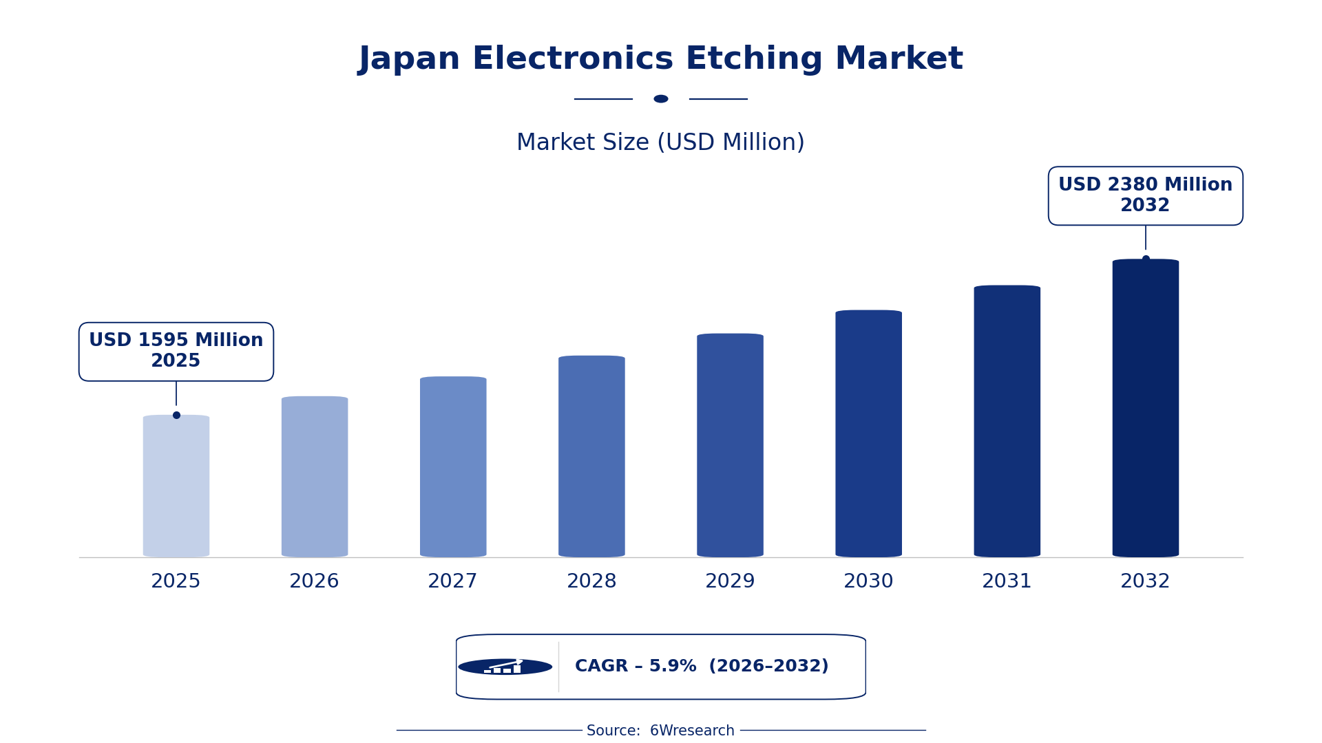
According to 6Wresearch internal database and industry insights, the Japan Electronics Etching Market was valued at USD 1,595 Million in 2025 and is projected to reach USD 2,380 Million by 2032, growing at a CAGR of approximately 5.9% during 2026–2032.
Japan Electronics Etching Market Highlights
| Report Metric | Details |
| Report Name | Japan Electronics Etching Market (2026-2032) |
| Market Size 2025 | USD 1,595 Million |
| Market Size 2032 | USD 2,380 Million |
| Absolute Growth 2025–2032 | USD 785 Million |
| CAGR 2026–2032 | 5.9% |
| Peak Annual Growth | 6.7% in 2027 |
| Forecast Period | 2026–2032 |
| Historical Data | 2022–2025 |
| Base Year | 2025 |
| Leading Etching Type, 2025 | Wet Etching (36% share) |
| Leading Etchant Used, 2025 | Acidic Solutions (40% share) |
| Leading Application, 2025 | PCB Fabrication (37% share) |
| Leading End User, 2025 | Semiconductor Labs (39% share) |
| Fastest-Growing Etching Type | Dry Etching (7.9% CAGR) |
| Fastest-Growing Etchant Used | Plasma (7.3% CAGR) |
| Fastest-Growing Application | IC Manufacturing (8.0% CAGR) |
| Fastest-Growing End User | Foundries (7.4% CAGR) |
| Growing Sector | semiconductor manufacturing |
| Key End Users | semiconductor labs, foundries, MEMS makers |
Japan Electronics Etching Market Year-wise Growth Rate and Key Drivers (2022–2032)
This graph illustrates the annual growth rates of the market from 2022 to 2032, highlighting a steady upward trajectory and projected market expansion over the forecast period.
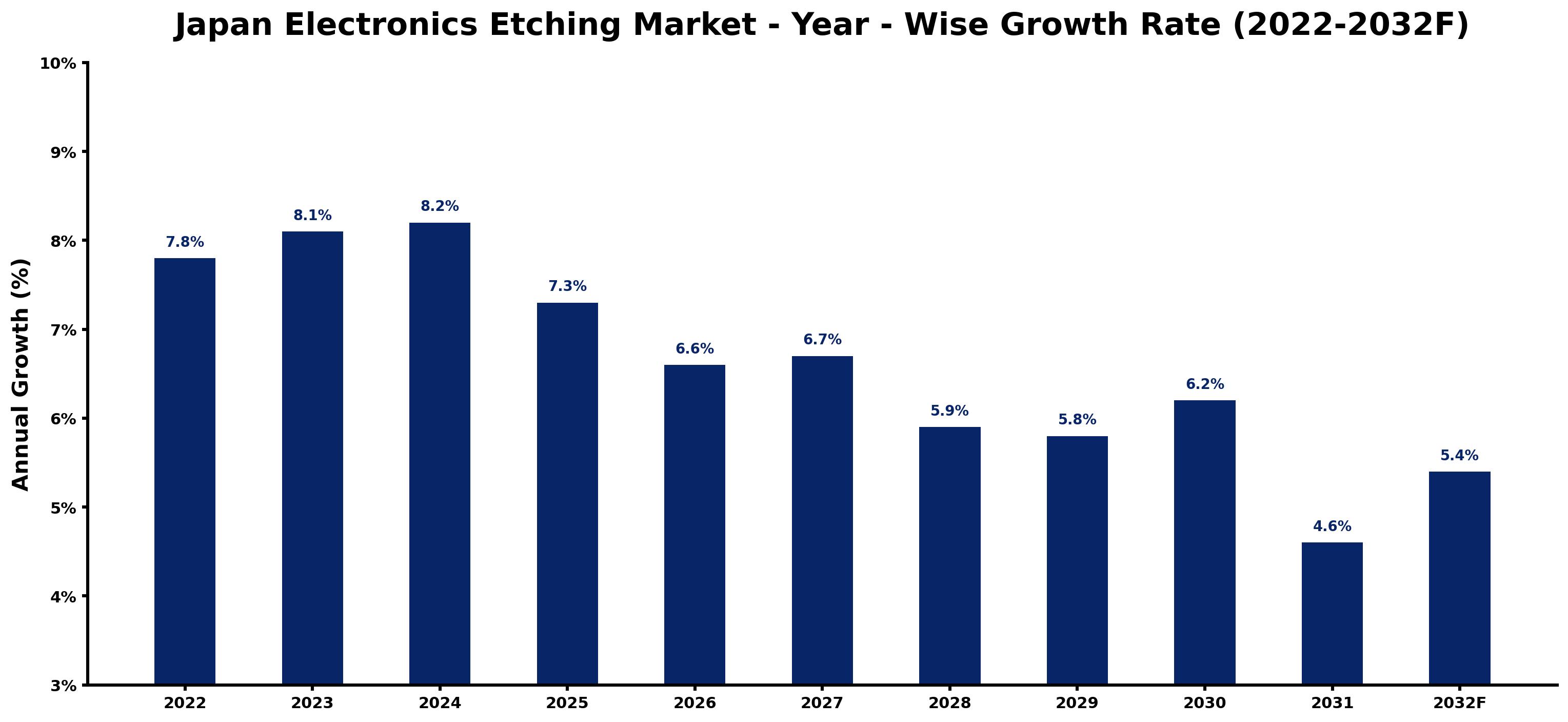
The yearly estimates that follow link every growth rate to its principal driver, so readers can see why the pace changed in each period.
| Year | Estimated Annual Growth (%) | Market Rationale |
| 2022 | 7.8 | The market experienced solid growth due to strong domestic semiconductor demand. |
| 2023 | 8.1 | Growth accelerated as semiconductor labs increased production capabilities. |
| 2024 | 8.2 | The market peaked as investments in advanced manufacturing technologies rose. |
| 2025 | 7.3 | Growth slowed as market conditions normalised after the peak. |
| 2026 | 6.6 | A further slowdown occurred as the market adjusted to new production levels. |
| 2027 | 6.7 | Demand is expected to rebound with increased orders from semiconductor foundries. |
| 2028 | 5.9 | Growth will continue to decelerate as the market stabilises. |
| 2029 | 5.8 | The market is projected to maintain stability with steady demand from key sectors. |
| 2030 | 6.2 | A slight uptick in growth is anticipated as new technologies are adopted. |
| 2031 | 4.6 | Growth will slow again as market saturation begins to take effect. |
| 2032 | 5.4 | Demand will rise as new applications for semiconductors emerge. |
Note: Market size estimations and growth projections presented in this report are based on 6Wresearch's proprietary forecasting methodology, utilizing the latest available industry data, government publications, and primary research inputs.
Japan Electronics Etching Market Synopsis
Electronics etching is essential in semiconductor manufacturing, involving the removal of material from substrates to create intricate patterns. The Japan Electronics Etching Market is expanding, driven by strong domestic demand and advanced manufacturing capabilities. In 2023, the government launched a 500 billion JPY programme to boost semiconductor production, which, along with over 200 semiconductor labs, is expected to stimulate demand for etching technologies.
Market Dynamics Impact Analysis (2026–2032)
| Factor | Type | Impact | Primary Segment Affected |
| Rising investments in semiconductor manufacturing capabilities | Driver | High | Wet Etching |
| Increased demand for advanced semiconductor devices | Driver | High | IC Manufacturing |
| Growing need for precision in semiconductor fabrication | Opportunity | High | Photo Etching |
| Expansion of semiconductor labs focusing on R&D | Opportunity | Medium | Semiconductor Labs |
| High operational costs for semiconductor foundries | Restraint | High | Foundries |
| Limited availability of skilled workforce in semiconductor sector | Restraint | Medium | MEMS Makers |
| Challenges in meeting stringent quality standards | Challenge | High | Dry Etching |
| Dependence on imported raw materials for etching processes | Challenge | Medium | Plasma |
Evaluation of Drivers in Japan Electronics Etching Market (2026–2032)
The table below links each growth driver to the segment it affects and the evidence for it.
| Drivers | Primary Segment Affected | Why It Matters (Evidence) |
| Increased government funding for semiconductor production | Wet Etching | The government allocated 500 billion JPY in 2023 to boost semiconductor manufacturing, leading to higher demand for etching services. |
| Growing production of MEMS devices | Microdevices | Japan is expected to produce 1 billion MEMS devices by 2025, increasing the need for precise etching technologies. |
| Rising adoption of ISO 9001 standards | Photo Etching | The prevalence of ISO 9001 in semiconductor manufacturing ensures quality, driving demand for reliable etching processes. |
| Expansion of semiconductor labs in Tokyo | Semiconductor Labs | With over 200 labs in Japan, the focus on advanced technologies boosts the demand for etching solutions. |
| Technological advancements in etching techniques | Dry Etching | Innovations in dry etching methods improve precision, attracting more orders from semiconductor manufacturers. |
This funding encourages expansion in production operations, driving demand for etching technologies. The production of MEMS devices is expected to reach 1 billion units by 2025, increasing the need for precise etching solutions. The widespread adoption of ISO 9001 standards in semiconductor manufacturing ensures quality, resulting in higher demand for reliable etching processes. Recent innovations in etching methods improve precision, attracting more orders from manufacturers seeking better outcomes.
Evaluation of Restraints in Japan Electronics Etching Market
These are the pressures that could keep growth below its potential.
| Market Restraint | Primary Segment Affected | Why It Matters (Evidence) |
| High operational costs affecting profitability | Foundries | Foundries face rising costs due to advanced technology investments, limiting their ability to expand etching services. |
| Limited availability of skilled workforce | MEMS Makers | The shortage of skilled workers in Japan's semiconductor sector hampers production efficiency and innovation. |
| Challenges in meeting stringent quality standards | Dry Etching | Manufacturers struggle to comply with rigorous quality requirements, impacting their competitiveness. |
| Dependence on imported raw materials | Plasma | Reliance on imports for key materials increases vulnerability to supply chain disruptions. |
| Market saturation in certain segments | IC Manufacturing | As the market matures, growth opportunities become limited, affecting long-term demand. |
Japan Electronics Etching Market Challenges
Japan's semiconductor manufacturing faces a critical supply issue, as reliance on imported chemicals can lead to delays in production schedules, impacting producers who require timely access to materials. A shortage of skilled workers in advanced etching techniques limits the capacity of manufacturers, with around 1,500 employees on average in foundries, resulting in slower output. Buyers encounter challenges due to price volatility of raw materials, which can increase production costs by 15%, squeezing their profit margins. Rising operational costs, linked to compliance with JIS Z 8401 standards, can escalate expenses for manufacturers, forcing them to pass on costs to buyers.
Trends in the Japan Electronics Etching Market
Buyers and suppliers in the Japan Electronics Etching Market are adjusting to the following trends.
- Shift from Wet to Dry Etching Technologies: Japan's semiconductor manufacturers are increasingly adopting dry etching technologies for their precision and efficiency. In 2023, dry etching accounted for a growing share of the market, reflecting a shift in production methods.
- Rising Demand for MEMS Devices: MEMS devices produced in Japan are projected to reach 1 billion units by 2025, indicating a growing demand for advanced etching processes. This trend is reshaping production in the semiconductor sector.
- Transition to Advanced Manufacturing Standards: The adoption of ISO 9001 standards in semiconductor manufacturing has been prevalent, ensuring quality and reliability. This shift has driven up demand for etching technologies that meet these rigorous standards.
- Growth in Semiconductor Labs in Tokyo: The Tokyo region is witnessing an increase in semiconductor labs, with over 200 focusing on advanced technologies. This growth is fostering innovation and driving demand for etching solutions.
Investment Opportunities in the Japan Electronics Etching Market
The following opportunities in the Japan Electronics Etching Market pair current demand with a clear way in.
- Tokyo Semiconductor Labs Expansion: The Tokyo region is expanding its semiconductor labs, creating a demand for advanced etching technologies. With over 200 labs, this growth represents a significant opportunity for suppliers.
- Investment in Precision Etching Solutions: With the semiconductor market valued at approximately 4 trillion JPY in 2022, there is a gap in precision etching solutions. Suppliers can target semiconductor foundries to meet this demand.
- Supply of Advanced Dry Etching Equipment: As dry etching technologies gain traction, suppliers can invest in advanced equipment. Foundries are seeking innovative solutions to enhance their production capabilities.
- Partnerships with Semiconductor Manufacturers: Collaborating with semiconductor manufacturers can facilitate entry into the market. Establishing joint ventures will help suppliers meet the growing demand for etching technologies.
Government Initiatives in the Japan Electronics Etching Market
The Semiconductor and Digital Industry Strategy, established by METI in June 2021, aims to secure domestic semiconductor manufacturing through various measures. This strategy has led to increased investments in production capabilities, improving the competitiveness of Japan's semiconductor industry. The Economic Security Promotion Act of 2022 further supports supply-chain resilience for critical products, ensuring a stable supply of materials for etching processes.
The Ministry of Economy, Trade and Industry (METI) oversees the approval of various semiconductor initiatives, including funding for research and development projects. In 2023, the government allocated 500 billion JPY to boost production, benefiting manufacturers and suppliers in the etching market. METI also monitors compliance with the PRTR Law and the Chemical Substances Control Law, ensuring that producers adhere to environmental regulations.
Future Insight of the Japan Electronics Etching Market
A policy-driven shift will reshape the semiconductor market by 2032, as the Japanese government allocates 300 billion JPY towards research and development initiatives. Suppliers will adopt new standards to ensure higher quality and consistency in production. Increased investment in advanced technologies will lead to etching techniques that improve efficiency and reduce waste. By 2025, MEMS device production is expected to reach 1 billion units, reflecting the heightened interest in advanced electronics.
Market Segmentation Analysis
Japan Electronics Etching Market report covers a detailed analysis of the following market segments:
By Etching Type – Wet Etching Leads, Dry Etching Expected to Grow Fastest
According to Saurav Kr Singh, Senior Research Analyst at 6Wresearch, Wet Etching took 36% of etching type revenue in 2025, more than any other category. Wet etching commands the largest share due to its prevalent use in semiconductor fabrication, particularly in Tokyo's semiconductor labs where precise material removal is vital. This method's reliability and effectiveness in achieving intricate designs solidify its status in the manufacturing landscape. Over 2026–2032, Dry Etching is expected to post the fastest growth, at a CAGR of 7.9%. The rapid growth of dry etching stems from its critical function in creating fine patterns on silicon wafers, increasingly demanded by advanced semiconductor technologies. As production requirements escalate, dry etching's adoption is set to rise, further expanding its market presence. Suppliers should enhance their dry etching offerings to address the growing demand in semiconductor manufacturing.
By Etchant Used – Acidic Solutions Lead, Plasma Expected to Grow Fastest
The largest etchant used category in 2025 was Acidic Solutions, at 40% of revenue. Acidic solutions lead the market as they are routinely utilised in wet etching processes, crucial for various semiconductor applications. Their effectiveness in material removal makes them a preferred choice among manufacturers, ensuring consistent performance in production. Plasma is projected to grow fastest, at a CAGR of 7.3% during 2026–2032. Plasma technology is witnessing rapid growth due to its capacity for high precision and control in dry etching processes, essential for modern semiconductor fabrication. As advancements continue, the adoption of plasma etching is expected to accelerate, reinforcing its market position. Buyers should explore sourcing advanced plasma etching technologies to maintain competitiveness in the semiconductor sector.
By Application – PCB Fabrication Leads, IC Manufacturing Expected to Grow Fastest
PCB Fabrication accounted for 37% of the market by application in 2025. PCB fabrication is the market leader due to its fundamental role in producing printed circuit boards, which are essential components of electronic devices. The substantial volume of PCB production in Japan's electronics industry underscores its importance and relevance. The quickest growth will come from IC Manufacturing, forecast to expand at a CAGR of 8.0% between 2026 and 2032. IC manufacturing is experiencing swift growth as it is a core process in the creation of integrated circuits, crucial for a diverse range of electronic applications. The rising demand for sophisticated ICs will further propel this segment's expansion, solidifying its market position. Suppliers must align their products to support the increasing requirements of IC manufacturing within the semiconductor sector.
By End User – Semiconductor Labs Lead, Foundries Expected to Grow Fastest
Semiconductor Labs held 39% of the Japan Electronics Etching Market by end user in 2025. Semiconductor labs are the primary users of etching technologies, concentrating on research and development to innovate new semiconductor materials and processes. Their significant investment in cutting-edge technologies reinforces their leading position in the market. Foundries are set to record the highest CAGR in this split, 7.4% over 2026–2032. Foundries are rapidly growing as major consumers of etching services for chip production, driven by the escalating demand for semiconductors across various sectors. This trend indicates a robust future for foundries, enhancing their importance in the market. Suppliers should focus on foundries to capitalise on the rising demand for etching services in chip production.
Key Attractiveness of the Report
- 10 Years of Market Numbers
- Historical Data Starting from 2022 to 2025
- Base Year 2025
- Forecast Data until 2032
- Key Performance Indicators Impacting the Market
- Major Upcoming Developments and Projects
Key Highlights of the Report:
- Japan Electronics Etching Market Outlook
- Market Size of Japan Electronics Etching Market, 2025
- Forecast of Japan Electronics Etching Market, 2032
- Historical Data and Forecast of Japan Electronics Etching Revenues & Volume for the Period 2022-2032F
- Japan Electronics Etching Market Trend Evolution
- Japan Electronics Etching Market Drivers and Challenges
- Japan Electronics Etching Price Trends
- Japan Electronics Etching Porter's Five Forces
- Japan Electronics Etching Industry Life Cycle
- Historical Data and Forecast of Japan Electronics Etching Market Revenues & Volume By Etching Type for the Period 2022-2032F
- Historical Data and Forecast of Japan Electronics Etching Market Revenues & Volume By Wet Etching for the Period 2022-2032F
- Historical Data and Forecast of Japan Electronics Etching Market Revenues & Volume By Dry Etching for the Period 2022-2032F
- Historical Data and Forecast of Japan Electronics Etching Market Revenues & Volume By Laser Etching for the Period 2022-2032F
- Historical Data and Forecast of Japan Electronics Etching Market Revenues & Volume By Photo Etching for the Period 2022-2032F
- Historical Data and Forecast of Japan Electronics Etching Market Revenues & Volume By Etchant Used for the Period 2022-2032F
- Historical Data and Forecast of Japan Electronics Etching Market Revenues & Volume By Acidic Solutions for the Period 2022-2032F
- Historical Data and Forecast of Japan Electronics Etching Market Revenues & Volume By Plasma for the Period 2022-2032F
- Historical Data and Forecast of Japan Electronics Etching Market Revenues & Volume By Focused Beam for the Period 2022-2032F
- Historical Data and Forecast of Japan Electronics Etching Market Revenues & Volume By Light Sensitive for the Period 2022-2032F
- Historical Data and Forecast of Japan Electronics Etching Market Revenues & Volume By Application for the Period 2022-2032F
- Historical Data and Forecast of Japan Electronics Etching Market Revenues & Volume By PCB Fabrication for the Period 2022-2032F
- Historical Data and Forecast of Japan Electronics Etching Market Revenues & Volume By IC Manufacturing for the Period 2022-2032F
- Historical Data and Forecast of Japan Electronics Etching Market Revenues & Volume By Microdevices for the Period 2022-2032F
- Historical Data and Forecast of Japan Electronics Etching Market Revenues & Volume By Sensors for the Period 2022-2032F
- Historical Data and Forecast of Japan Electronics Etching Market Revenues & Volume By End User for the Period 2022-2032F
- Historical Data and Forecast of Japan Electronics Etching Market Revenues & Volume By Semiconductor Labs for the Period 2022-2032F
- Historical Data and Forecast of Japan Electronics Etching Market Revenues & Volume By Foundries for the Period 2022-2032F
- Historical Data and Forecast of Japan Electronics Etching Market Revenues & Volume By MEMS Makers for the Period 2022-2032F
- Historical Data and Forecast of Japan Electronics Etching Market Revenues & Volume By Optical Component Firms for the Period 2022-2032F
- Japan Electronics Etching Import Export Trade Statistics
- Market Opportunity Assessment By Etching Type
- Market Opportunity Assessment By Etchant Used
- Market Opportunity Assessment By Application
- Market Opportunity Assessment By End User
- Japan Electronics Etching Top Companies Market Share
- Japan Electronics Etching Competitive Benchmarking By Technical and Operational Parameters
- Japan Electronics Etching Company Profiles
- Japan Electronics Etching Key Strategic Recommendations
Market Covered
The report covers the following segments.
By Etching Type
- Wet Etching
- Dry Etching
- Laser Etching
- Photo Etching
By Etchant Used
- Acidic Solutions
- Plasma
- Focused Beam
- Light Sensitive
By Application
- PCB Fabrication
- IC Manufacturing
- Microdevices
- Sensors
By End User
- Semiconductor Labs
- Foundries
- MEMS Makers
- Optical Component Firms