Japan Semiconductor Coating Market Size & Growth Rate
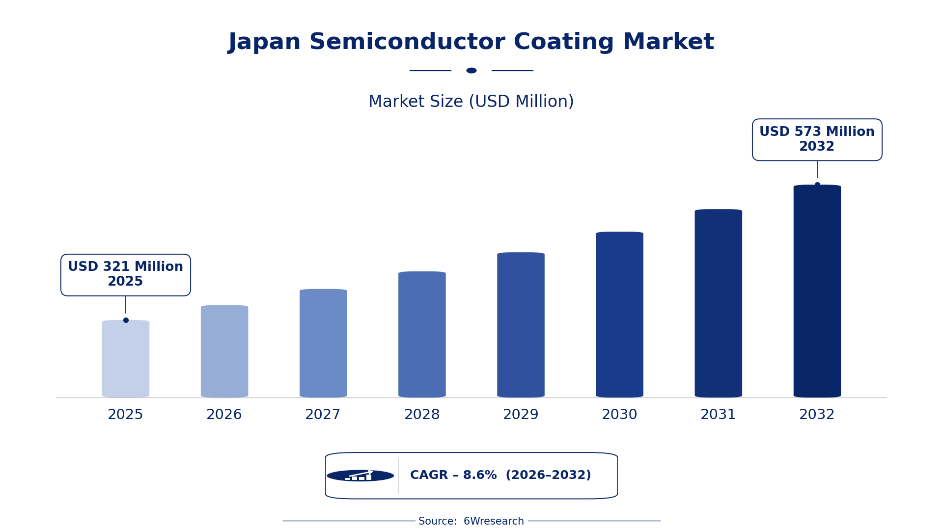
According to 6Wresearch internal database and industry insights, the Japan Semiconductor Coating Market was valued at USD 321 Million in 2025 and is projected to reach USD 573 Million by 2032, growing at a CAGR of approximately 8.6% during 2026–2032.
Japan Semiconductor Coating Market Highlights
| Report Metric | Details |
| Report Name | Japan Semiconductor Coating Market (2026-2032) |
| Market Size 2025 | USD 321 Million |
| Market Size 2032 | USD 573 Million |
| Absolute Growth 2025–2032 | USD 252 Million |
| CAGR 2026–2032 | 8.6% |
| Peak Annual Growth | 9.5% in 2028 |
| Forecast Period | 2026–2032 |
| Historical Data | 2022–2025 |
| Base Year | 2025 |
| Leading Coating Type, 2025 | Anti-Reflective Coating (47% share) |
| Leading Application Stage, 2025 | Lithography (44% share) |
| Leading Method Used, 2025 | Spin Coating (43% share) |
| Leading End User, 2025 | Foundries (40% share) |
| Fastest-Growing Coating Type | Passivation Coating (12.6% CAGR) |
| Fastest-Growing Application Stage | Final Protection Layer (11.5% CAGR) |
| Fastest-Growing Method Used | CVD (12.0% CAGR) |
| Fastest-Growing End User | IDM/Packaging Plants (11.8% CAGR) |
| Growing Sector | automotive semiconductor applications |
| Key End Users | foundries, device fabricators, IDM/packaging plants |
Japan Semiconductor Coating Market Year-wise Growth Rate and Key Drivers (2022–2032)
This graph illustrates the annual growth rates of the market from 2022 to 2032, highlighting a steady upward trajectory and projected market expansion over the forecast period.
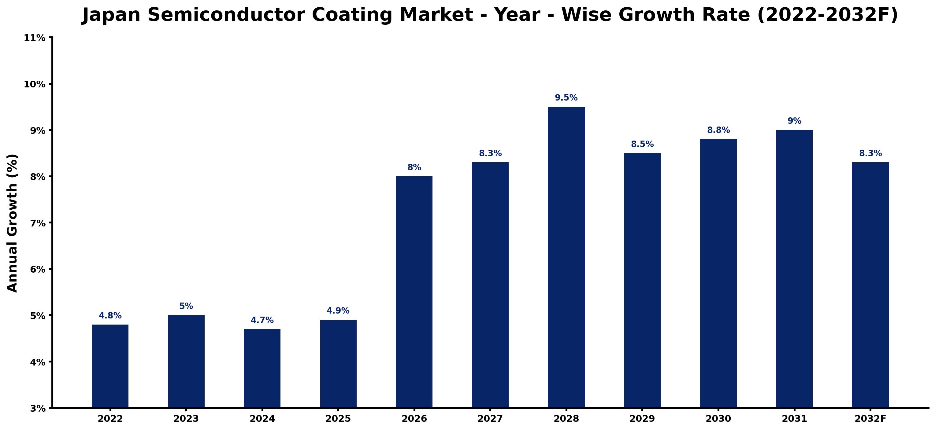
The following figures match every annual growth estimate with the main market development of that year, giving the reasoning behind each rise or slowdown.
| Year | Estimated Annual Growth (%) | Market Rationale |
| 2022 | 4.8 | The market showed steady growth due to strong domestic demand from foundries. |
| 2023 | 5.0 | Growth accelerated as semiconductor production increased by 5% in the country. |
| 2024 | 4.7 | The growth rate slowed slightly as supply chain adjustments took place. |
| 2025 | 4.9 | Demand rose again as investments in advanced packaging technologies gained traction. |
| 2026 | 8.0 | Growth is expected to rise as domestic production capabilities improve by 2025. |
| 2027 | 8.3 | The market will continue to expand with increasing adoption of CVD methods. |
| 2028 | 9.5 | A peak growth rate is anticipated as technology innovations drive demand. |
| 2029 | 8.5 | Growth will slow as the market stabilises after reaching its peak. |
| 2030 | 8.8 | Demand is projected to rise again as new semiconductor applications emerge. |
| 2031 | 9.0 | Market growth will continue as foundries expand their production capabilities. |
| 2032 | 8.3 | The growth rate will moderate but remain positive as the industry matures. |
Note: Market size estimations and growth projections presented in this report are based on 6Wresearch's proprietary forecasting methodology, utilizing the latest available industry data, government publications, and primary research inputs.
Japan Semiconductor Coating Market Synopsis
Semiconductor coating involves applying materials to semiconductor surfaces to improve performance and protect against environmental damage. The Japan Semiconductor Coating Market is growing due to strong demand from local foundries and device fabricators, with the semiconductor market valued at approximately 4 trillion yen as of 2023. The rise in advanced packaging technologies in the automotive sector also contributes to this growth. Initiatives from the Ministry of Economy, Trade and Industry support innovation in semiconductor technology, creating a competitive environment for manufacturers.
Market Dynamics Impact Analysis (2026–2032)
| Factor | Type | Impact | Primary Segment Affected |
| Strong domestic demand from foundries drives the need for high-quality coatings. | Driver | High | Anti-Reflective Coating |
| The increasing complexity of semiconductor devices creates opportunities for advanced coatings. | Opportunity | High | Passivation Coating |
| Regulatory compliance with the JIS Z 8730 standard can limit production capabilities. | Restraint | High | Dielectric Coating |
| Limited availability of skilled workforce affects production efficiency. | Challenge | High | Spin Coating |
| The rise in automotive semiconductor applications boosts demand for advanced coatings. | Driver | Medium | Final Protection Layer |
| Investment in semiconductor manufacturing facilities presents opportunities for suppliers. | Opportunity | Medium | CVD |
| High costs associated with advanced coating technologies can deter smaller manufacturers. | Restraint | Medium | Conformal Coating |
| Compliance with chemical regulations can complicate material sourcing. | Challenge | Medium | Passivation Coating |
Evaluation of Drivers in Japan Semiconductor Coating Market (2026–2032)
Below are the drivers that matter most for revenue growth, with supporting evidence.
| Drivers | Primary Segment Affected | Why It Matters (Evidence) |
| Increased semiconductor production in the Tokyo region boosts demand for coatings. | Anti-Reflective Coating | Numerous foundries in the Tokyo area lead to higher coating requirements. |
| The adoption of advanced packaging technologies in automotive applications drives demand. | Final Protection Layer | The growth in the automotive sector necessitates reliable semiconductor devices. |
| The rise in semiconductor exports encourages local manufacturers to improve coating quality. | Dielectric Coating | Exports reached approximately 1.5 trillion yen, prompting higher production standards. |
| Government support for innovation in coating technologies enhances market potential. | CVD | This initiative aims to strengthen domestic production capabilities by 2025. |
| Local foundries are investing in new equipment to meet rising demand for coatings. | Spin Coating | The installed base of semiconductor manufacturing equipment exceeds 100,000 units. |
Volumes grow on the back of strong domestic demand, particularly from local foundries and device fabricators. The semiconductor market is valued at approximately 4 trillion yen, prompting significant investments in advanced coating technologies. Exports reached around 1.5 trillion yen, compelling local manufacturers to enhance their coating quality. The automotive sector's growth necessitates reliable semiconductor devices, which increases the need for effective coatings. As production capabilities improve, demand for innovative coating solutions is expected to rise.
Evaluation of Restraints in Japan Semiconductor Coating Market
The following restraints limit how fast demand can grow.
| Market Restraint | Primary Segment Affected | Why It Matters (Evidence) |
| Compliance with the JIS Z 8730 standard can limit production capabilities. | Dielectric Coating | Manufacturers must ensure their coatings meet strict quality regulations. |
| High costs associated with advanced coating technologies can deter smaller manufacturers. | Conformal Coating | Smaller firms struggle to invest in sophisticated coating methods. |
| Limited availability of skilled workforce affects production efficiency. | Spin Coating | A shortage of trained personnel can slow down manufacturing processes. |
| Regulatory compliance with chemical laws complicates material sourcing. | Passivation Coating | Manufacturers must navigate complex regulations, increasing operational costs. |
| Market fluctuations in raw material prices can impact profitability. | Anti-Reflective Coating | Volatility in material costs can strain budgets for manufacturers. |
Japan Semiconductor Coating Market Challenges
Delays in project timelines for producers stem from a shortage of skilled workers in semiconductor coating techniques, potentially extending schedules by up to six months. Compliance with the JIS Z 8730 standard incurs significant quality assurance costs, estimated at around 500 million yen annually for producers. Supply chain disruptions have lengthened lead times for raw materials, prompting buyers to maintain excess inventory valued at approximately 200 million yen. Intense competition from international markets pressures local producers to reduce prices, which may lead to a 10% revenue decline for smaller firms.
Trends in the Japan Semiconductor Coating Market
Several trends are reshaping the Japan Semiconductor Coating Market; the most important are set out below.
- Shift in Focus to Advanced Packaging Technologies: The Tokyo region is experiencing a shift towards advanced packaging technologies, particularly in automotive applications, with a reported 5% increase in semiconductor production in 2023. This trend highlights a growing need for effective coatings to enhance device performance.
- Transition from Traditional to Modern Coating Methods: The semiconductor industry is transitioning from traditional coating methods to modern techniques such as CVD and spin coating. The adoption of these methods is expected to rise, driven by the demand for higher quality and performance in semiconductor devices.
- Emergence of Dielectric Coatings in Semiconductor Applications: Dielectric coatings are gaining importance for electrical insulation in semiconductor devices. The demand for these coatings is anticipated to grow significantly as semiconductor device complexity increases.
- Increased Adoption of Regulatory Standards: The introduction of the Economic Security Promotion Act in 2022 has led to greater compliance with regulatory standards in semiconductor production. This shift encourages manufacturers to invest in more sustainable coating technologies.
Investment Opportunities in the Japan Semiconductor Coating Market
The openings below show where demand in the Japan Semiconductor Coating Market is visible and how suppliers can enter.
- Investment in Semiconductor Manufacturing Facilities: The Tokyo region is currently witnessing substantial investments in semiconductor manufacturing facilities, with the installed base exceeding 100,000 units. Suppliers can enter this market by forming joint ventures with local foundries.
- Growing Demand for Advanced Coatings: The rise in automotive semiconductor applications presents a prime opportunity for suppliers of advanced coatings. The anticipated growth in this sector creates a demand for reliable products that improve performance.
- Expansion of CVD Technology: With a projected CAGR of 12.0% for CVD coatings, there is a strong opportunity for suppliers to invest in this technology. Collaborating with device fabricators in the Tokyo region can facilitate market entry.
- Focus on Compliance with Quality Standards: As the JIS Z 8730 standard governs semiconductor coatings, manufacturers have the opportunity to develop compliant products. Engaging with local regulatory bodies can help ensure adherence to these standards.
Government Initiatives in the Japan Semiconductor Coating Market
The Semiconductor and Digital Industry Strategy, established by METI in June 2021, includes measures to strengthen domestic semiconductor manufacturing. This involves funding for technology innovation and infrastructure development, targeting improvements in production capabilities by 2025. Such initiatives directly impact producers of semiconductor coatings by promoting advancements in coating technologies and improving overall production efficiency.
The Ministry of Economy, Trade and Industry implements the Semiconductor and Digital Industry Strategy, providing funding for projects that enhance semiconductor production. Local foundries benefit from these initiatives, as they receive support for upgrading equipment and refining coating technologies, which is essential for meeting market demands.
Future Insight of the Japan Semiconductor Coating Market
Technological advancements in semiconductor coatings will reshape demand by 2032, especially as the automotive sector seeks specialised materials. The Ministry of Economy, Trade and Industry's innovation support programme is expected to boost domestic production capabilities by 15%. The rise of electric vehicles will create demand for coatings designed for specific automotive applications. By 2025, initiatives focused on strengthening local production will establish a more dependable supply chain for buyers and suppliers.
Market Segmentation Analysis
Japan Semiconductor Coating Market report covers a detailed analysis of the following market segments:
By Coating Type – Anti-Reflective Coating Leads, Passivation Coating Expected to Grow Fastest
According to Saurav Kr Singh, Senior Research Analyst at 6Wresearch, Anti-Reflective Coating took 47% of coating type revenue in 2025, more than any other category. Anti-Reflective Coating commands the largest share due to its critical role in enhancing light absorption during photolithography, a fundamental process in semiconductor manufacturing. Its widespread use in facilities across the Tokyo region illustrates its importance in supporting local foundries. Passivation Coating is set to record the highest CAGR in this split, 12.6% over 2026–2032. Passivation Coating is experiencing rapid growth as it provides essential surface protection and reliability for semiconductor devices, aligning with the industry's focus on longevity. The support from the Ministry of Economy, Trade and Industry for technology innovation is further boosting this demand. Suppliers should focus on expanding their passivation coating offerings to cater to the increasing needs of manufacturers.
By Application Stage – Lithography Leads, Final Protection Layer Expected to Grow Fastest
With 44% of application stage revenue in 2025, Lithography was the largest category. Lithography holds the leading position in the application stage as it is a crucial step in semiconductor manufacturing, ensuring the precise patterning of circuits on wafers. The high frequency of lithography processes in Japan's semiconductor foundries highlights its vital role in the market. Final Protection Layer is projected to grow fastest, at a CAGR of 11.5% during 2026–2032. Final Protection Layer is witnessing the fastest growth due to its essential function in safeguarding completed semiconductor devices from environmental damage. The rising demand for advanced packaging technologies, particularly in the automotive sector, is driving this trend. Buyers will increasingly prioritise reliable solutions for final protection layers to ensure the durability of their semiconductor products.
By Method Used – Spin Coating Leads, CVD Expected to Grow Fastest
The largest method used category in 2025 was Spin Coating, at 43% of revenue. Spin Coating is the leading method for applying coatings, widely recognised for its efficiency and effectiveness in semiconductor manufacturing processes. Its prevalent use across Japan's extensive installed base of over 100,000 units of manufacturing equipment underscores its established market presence. Over 2026–2032, CVD is expected to post the fastest growth, at a CAGR of 12.0%. CVD is rapidly growing as it is a common method for depositing thin films, which are essential for advanced semiconductor applications. The industry's push for innovation and improved production capabilities is accelerating the adoption of CVD techniques. Suppliers must invest in CVD technology to take advantage of its increasing popularity among manufacturers.
By End User – Foundries Lead, IDM/Packaging Plants Expected to Grow Fastest
Foundries held 40% of the Japan Semiconductor Coating Market by end user in 2025. Foundries are the largest end user group of semiconductor coatings, as they are essential for producing a wide range of semiconductor devices. The concentration of major foundries in Japan, especially in the Tokyo region, reinforces their dominant position in the market. The quickest growth will come from IDM/Packaging Plants, forecast to expand at a CAGR of 11.8% between 2026 and 2032. IDM/Packaging Plants are experiencing the fastest growth due to their significant role in packaging processes, which are becoming increasingly vital in the semiconductor supply chain. The shift towards advanced packaging technologies is driving this demand. Suppliers should tailor their products to meet the specific requirements of IDM/Packaging Plants to capture this expanding market segment.
Key Attractiveness of the Report
- 10 Years of Market Numbers
- Historical Data Starting from 2022 to 2025
- Base Year 2025
- Forecast Data until 2032
- Key Performance Indicators Impacting the Market
- Major Upcoming Developments and Projects
Key Highlights of the Report:
- Japan Semiconductor Coating Market Outlook
- Market Size of Japan Semiconductor Coating Market, 2025
- Forecast of Japan Semiconductor Coating Market, 2032
- Historical Data and Forecast of Japan Semiconductor Coating Revenues & Volume for the Period 2022-2032F
- Japan Semiconductor Coating Market Trend Evolution
- Japan Semiconductor Coating Market Drivers and Challenges
- Japan Semiconductor Coating Price Trends
- Japan Semiconductor Coating Porter's Five Forces
- Japan Semiconductor Coating Industry Life Cycle
- Historical Data and Forecast of Japan Semiconductor Coating Market Revenues & Volume By Coating Type for the Period 2022-2032F
- Historical Data and Forecast of Japan Semiconductor Coating Market Revenues & Volume By Anti-Reflective Coating for the Period 2022-2032F
- Historical Data and Forecast of Japan Semiconductor Coating Market Revenues & Volume By Passivation Coating for the Period 2022-2032F
- Historical Data and Forecast of Japan Semiconductor Coating Market Revenues & Volume By Conformal Coating for the Period 2022-2032F
- Historical Data and Forecast of Japan Semiconductor Coating Market Revenues & Volume By Dielectric Coating for the Period 2022-2032F
- Historical Data and Forecast of Japan Semiconductor Coating Market Revenues & Volume By Application Stage for the Period 2022-2032F
- Historical Data and Forecast of Japan Semiconductor Coating Market Revenues & Volume By Lithography for the Period 2022-2032F
- Historical Data and Forecast of Japan Semiconductor Coating Market Revenues & Volume By Final Protection Layer for the Period 2022-2032F
- Historical Data and Forecast of Japan Semiconductor Coating Market Revenues & Volume By Wafer Surfaces for the Period 2022-2032F
- Historical Data and Forecast of Japan Semiconductor Coating Market Revenues & Volume By Isolation Layer for the Period 2022-2032F
- Historical Data and Forecast of Japan Semiconductor Coating Market Revenues & Volume By Method Used for the Period 2022-2032F
- Historical Data and Forecast of Japan Semiconductor Coating Market Revenues & Volume By Spin Coating for the Period 2022-2032F
- Historical Data and Forecast of Japan Semiconductor Coating Market Revenues & Volume By CVD for the Period 2022-2032F
- Historical Data and Forecast of Japan Semiconductor Coating Market Revenues & Volume By Spray or Dip for the Period 2022-2032F
- Historical Data and Forecast of Japan Semiconductor Coating Market Revenues & Volume By Sputtering for the Period 2022-2032F
- Historical Data and Forecast of Japan Semiconductor Coating Market Revenues & Volume By End User for the Period 2022-2032F
- Historical Data and Forecast of Japan Semiconductor Coating Market Revenues & Volume By Foundries for the Period 2022-2032F
- Historical Data and Forecast of Japan Semiconductor Coating Market Revenues & Volume By IDM/Packaging Plants for the Period 2022-2032F
- Historical Data and Forecast of Japan Semiconductor Coating Market Revenues & Volume By Device Fabricators for the Period 2022-2032F
- Historical Data and Forecast of Japan Semiconductor Coating Market Revenues & Volume By Advanced Packaging Units for the Period 2022-2032F
- Japan Semiconductor Coating Import Export Trade Statistics
- Market Opportunity Assessment By Coating Type
- Market Opportunity Assessment By Application Stage
- Market Opportunity Assessment By Method Used
- Market Opportunity Assessment By End User
- Japan Semiconductor Coating Top Companies Market Share
- Japan Semiconductor Coating Competitive Benchmarking By Technical and Operational Parameters
- Japan Semiconductor Coating Company Profiles
- Japan Semiconductor Coating Key Strategic Recommendations
Market Covered
Segments analysed in this report are listed below.
By Coating Type
- Anti-Reflective Coating
- Passivation Coating
- Conformal Coating
- Dielectric Coating
By Application Stage
- Lithography
- Final Protection Layer
- Wafer Surfaces
- Isolation Layer
By Method Used
- Spin Coating
- CVD
- Spray or Dip
- Sputtering
By End User
- Foundries
- IDM/Packaging Plants
- Device Fabricators
- Advanced Packaging Units