India Thin Film Deposition Market Size & Growth Rate
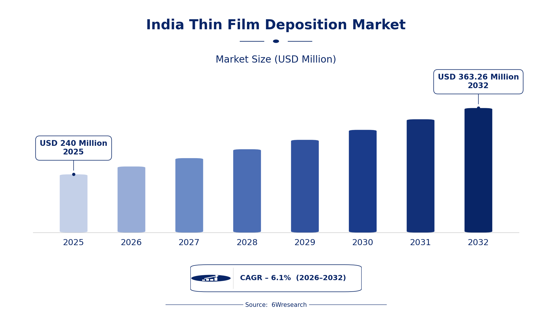
According to 6Wresearch internal database and industry insights, the India Thin Film Deposition Market was valued at USD 240.0 million in 2025 and is projected to reach USD 363.26 million by 2032, growing at a CAGR of approximately 6.1% during 2026–2032.
India Thin Film Deposition Market Highlights
| Report Metric | Details |
| Report Name | India Thin Film Deposition Market |
| Market Size 2025 | USD 240.0 million |
| Market Size 2032 | USD 363.26 million |
| Absolute Growth 2025–2032 | USD 123.26 million |
| CAGR 2026–2032 | 6.1% |
| Peak Annual Growth | 8.5% in 2028 |
| Forecast Period | 2026–2032 |
| Historical Data | 2022–2025 |
| Base Year | 2025 |
| Leading Deposition Type, 2025 | Chemical Vapor Deposition (CVD) (34% share) |
| Leading Material Type, 2025 | Metals (47% share) |
| Leading Technology Used, 2025 | Sputtering (47% share) |
| Leading End User, 2025 | Semiconductor Foundries (40% share) |
| Fastest-Growing Deposition Type | Atomic Layer Deposition (ALD) (8.0% CAGR) |
| Fastest-Growing Material Type | Nanolayers (8.8% CAGR) |
| Fastest-Growing Technology Used | Plasma-Enhanced (7.5% CAGR) |
| Fastest-Growing End User | Solar Cell Firms (7.1% CAGR) |
| Growing Sector | Semiconductor Manufacturing |
| Key End Users | Semiconductor Foundries, Solar Cell Firms, Display Panel Producers, R&D Labs |
India Thin Film Deposition Market Year-wise Growth Rate and Key Drivers (2022–2032)
This graph illustrates the annual growth rates of the market from 2022 to 2032, highlighting a steady upward trajectory and projected market expansion over the forecast period.
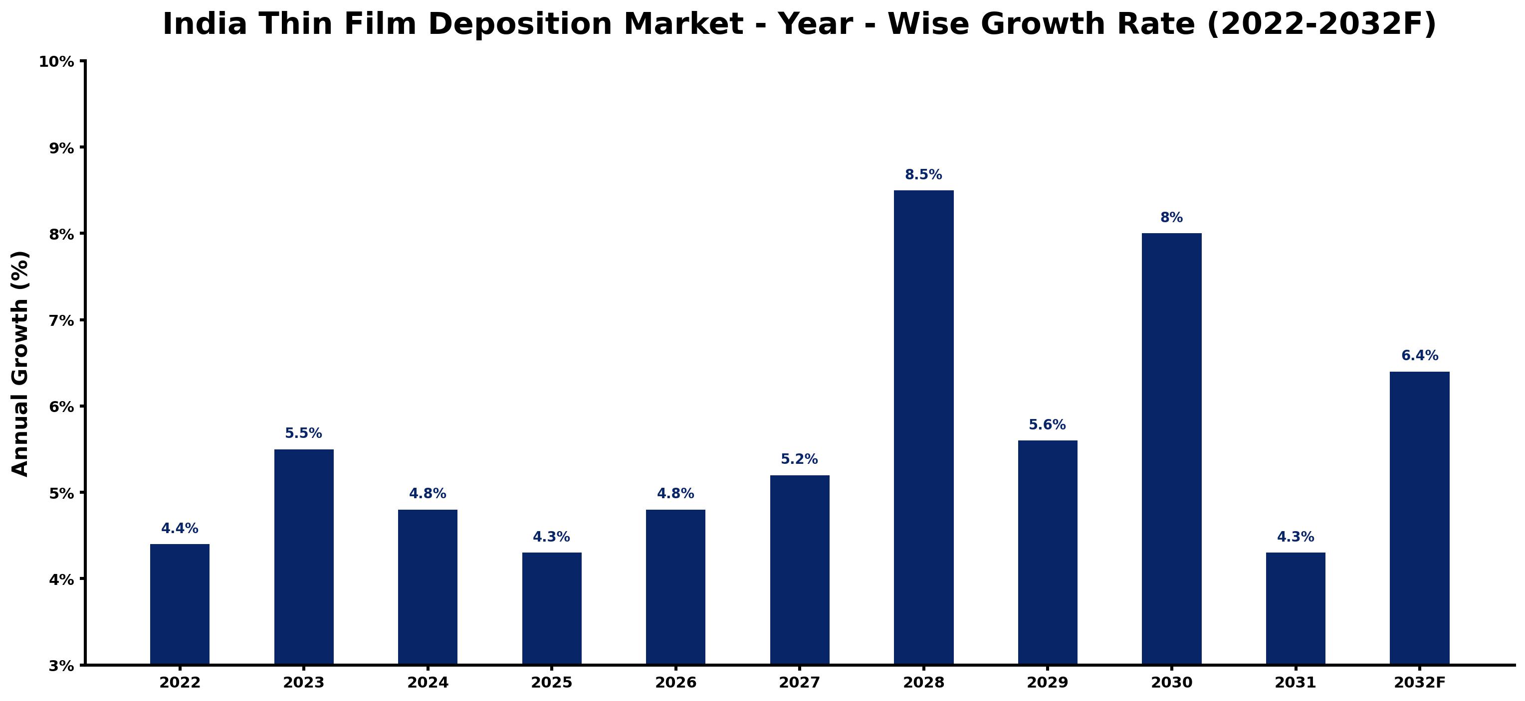
Each row of the following table gives one year's estimated growth and the event or demand shift that explains it.
| Year | Estimated Annual Growth (%) | Market Rationale |
| 2022 | 4.4 | The market experienced steady growth, driven by increasing demand from semiconductor foundries. |
| 2023 | 5.5 | Growth accelerated due to the expanding semiconductor market, projected to reach $63 billion by 2026. |
| 2024 | 4.8 | A slight slowdown occurred as the market adjusted to previous growth levels. |
| 2025 | 4.3 | Continued growth was observed, although at a slower pace compared to earlier years. |
| 2026 | 4.8 | The market is expected to rebound with renewed interest in advanced manufacturing technologies. |
| 2027 | 5.2 | Growth will continue as semiconductor foundries expand their production capabilities. |
| 2028 | 8.5 | A surge in demand is anticipated, driven by the Semiconductor Mission's initiatives. |
| 2029 | 5.6 | The market will experience a slowdown as growth stabilises after the peak. |
| 2030 | 8.0 | Renewed momentum is expected as investments in solar technologies increase. |
| 2031 | 4.3 | Growth will decelerate, reflecting adjustments following previous high rates. |
| 2032 | 6.4 | A resurgence in demand is expected as the semiconductor ecosystem matures. |
Note: Market size estimations and growth projections presented in this report are based on 6Wresearch's proprietary forecasting methodology, utilizing the latest available industry data, government publications, and primary research inputs.
India Thin Film Deposition Market Synopsis
Thin Film Deposition technologies in India apply thin layers of materials, primarily in semiconductor and solar industries. This technology is crucial for manufacturing semiconductors, display panels, and solar cells. The India Thin Film Deposition Market is growing due to rising domestic demand, particularly from semiconductor foundries and solar cell manufacturers. Investment in advanced manufacturing technologies is driving further purchases, supported by the Electronics Policy 2020 and the Semiconductor Mission, which boost domestic capabilities.
Market Dynamics Impact Analysis (2026–2032)
| Factor | Type | Impact | Primary Segment Affected |
| Increasing domestic semiconductor production | Driver | High | Physical Vapor Deposition (PVD) |
| Growing solar capacity driving demand for thin films | Driver | High | Chemical Vapor Deposition (CVD) |
| Development of advanced manufacturing technologies | Opportunity | High | Atomic Layer Deposition (ALD) |
| Expansion of semiconductor foundries in Karnataka | Opportunity | Medium | Semiconductor Foundries |
| High initial investment costs for advanced technologies | Restraint | High | Sputtering |
| Limited awareness of thin film technologies among new entrants | Restraint | Medium | Display Panel Producers |
| Supply chain disruptions affecting material availability | Challenge | High | Solar Cell Firms |
| Approval delays for new technologies and processes | Challenge | Medium | R&D Labs |
Evaluation of Drivers in India Thin Film Deposition Market (2026–2032)
Below mentioned are some major drivers and their influence on market dynamics.
| Drivers | Primary Segment Affected | Why It Matters (Evidence) |
| Surge in semiconductor manufacturing investments | Chemical Vapor Deposition (CVD) | India's semiconductor market is projected to reach $63 billion by 2026, prompting increased demand for thin film technologies. |
| Expansion of solar energy projects | Sputtering | India's solar capacity reached 40 GW in 2023, driving demand for thin film deposition in solar cells. |
| Government initiatives supporting electronics manufacturing | Atomic Layer Deposition (ALD) | The Semiconductor Mission aims to establish a semiconductor manufacturing base with a budget of $10 billion over six years. |
| Growth in R&D activities for semiconductor technologies | Physical Vapor Deposition (PVD) | With over 1,000 R&D labs focusing on semiconductors, demand for thin film technologies is set to rise. |
| Investment in electronics manufacturing infrastructure | Electrochemical Deposition | The Electronics Manufacturing Cluster Scheme supports infrastructure development, enhancing production capacity for thin film technologies. |
In 2023, India's solar capacity reached 40 GW, further boosting demand for deposition methods. With over 1,000 R&D labs focusing on semiconductor technologies, the market is set to grow. Infrastructure improvements through the Electronics Manufacturing Cluster Scheme are supporting the production of thin films across various applications.
Evaluation of Restraints in India Thin Film Deposition Market
The main factors holding the market back are set out below.
| Market Restraint | Primary Segment Affected | Why It Matters (Evidence) |
| High costs associated with advanced deposition technologies | Sputtering | Initial investments for advanced technologies can be prohibitive, limiting entry for smaller firms. |
| Lack of awareness about thin film applications | Display Panel Producers | New entrants may struggle to understand the benefits of thin film technologies, hindering adoption. |
| Supply chain disruptions for key materials | Solar Cell Firms | Global supply chain issues can lead to material shortages, affecting production timelines and costs. |
| Regulatory approval delays for new technologies | R&D Labs | Long approval processes can slow down the introduction of new thin film technologies, delaying market entry. |
| Limited access to skilled workforce in advanced manufacturing | Atomic Layer Deposition (ALD) | A shortage of trained professionals can restrict the growth of advanced thin film applications. |
India Thin Film Deposition Market Challenges
The India Thin Film Deposition market is hindered by high production costs, primarily due to expensive raw materials, which can increase prices for buyers by 20%. Supply chain disruptions are prevalent, causing delays that can extend lead times for producers by up to four weeks. A shortage of skilled workers in advanced manufacturing techniques limits suppliers' ability to meet rising demand, affecting their production capabilities. Buyers face challenges with regulatory compliance, as adhering to the Bureau of Indian Standards can add an average of three months to project timelines.
Trends in the India Thin Film Deposition Market
Several trends are reshaping the India Thin Film Deposition Market; the most important are set out below.
- Shift in Focus to Advanced Semiconductor Manufacturing: Semiconductor foundries are increasingly adopting advanced thin film deposition techniques to improve production efficiency. The Semiconductor Mission aims to establish a semiconductor base with an investment of $10 billion over six years.
- Growth of Solar Energy Applications: Solar cell manufacturers are rapidly integrating thin film technologies to enhance efficiency. India's solar capacity reached 40 GW in 2023, indicating a strong market for innovative deposition methods.
- Adoption of Plasma-Enhanced Deposition Techniques: Plasma-enhanced deposition methods are gaining traction among semiconductor manufacturers for their efficiency. This technology is anticipated to grow at a CAGR of 7.5% from 2026 to 2032, reflecting increasing adoption.
- Emergence of Nanolayers in Electronics: Nanolayers are becoming increasingly important in advanced electronic components, driving demand for precise deposition techniques. The segment is expected to grow at a CAGR of 8.8% from 2026 to 2032, highlighting its significance.
Investment Opportunities in the India Thin Film Deposition Market
Some of the investment opportunities in the India Thin Film Deposition Market are mentioned below.
- Timing for Investment in Semiconductor Technologies: With the semiconductor market expanding rapidly, investing in thin film deposition technologies is timely. Collaborating with semiconductor foundries in Karnataka can yield substantial returns for investors.
- Infrastructure Development in Electronics Manufacturing: The Electronics Manufacturing Cluster Scheme supports infrastructure for electronics production. Investing in this sector can yield significant returns, particularly in states like Telangana, which are prioritising technology development.
- Supply of Advanced Thin Film Technologies: There is a growing need for advanced thin film deposition technologies in India. Collaborating with R&D labs can facilitate entry into this expanding market, particularly in regions with strong semiconductor activities.
- Entry through Local Partnerships: Establishing joint ventures with local semiconductor firms can enhance market access. This approach is particularly effective in Karnataka, a hub for semiconductor manufacturing, providing opportunities for collaboration.
Government Initiatives in the India Thin Film Deposition Market
The Electronics Policy 2020, initiated by the Ministry of Electronics and Information Technology, aims to enhance domestic manufacturing capabilities and reduce import dependency. This policy encourages local production of thin film technologies, providing incentives for manufacturers to invest in advanced processes. The Semiconductor Mission, launched in 2021, seeks to establish a semiconductor manufacturing base with a budget of $10 billion over six years. This funding supports the development of infrastructure and technology, promoting growth in the thin film deposition market.
The Electronics Manufacturing Cluster Scheme, implemented by the Ministry of Electronics, supports the development of infrastructure for electronics manufacturing across states. This scheme provides financial assistance to firms establishing manufacturing facilities, enabling them to improve production capabilities. Additionally, the National Institute of Electronics and Information Technology offers training in thin film technologies, ensuring a skilled workforce for the industry. These initiatives strengthen the thin film deposition market by promoting local production and innovation.
Future Insight of the India Thin Film Deposition Market
The India Thin Film Deposition market will experience significant transformation by 2032, primarily driven by the semiconductor sector's anticipated growth. The Electronics Manufacturing Cluster Scheme will enhance infrastructure, facilitating smoother operations for suppliers. Investment in advanced manufacturing technologies will improve production efficiency, allowing buyers to obtain high-quality products more readily. The government's Semiconductor Mission will create a robust ecosystem, encouraging innovation and attracting a skilled workforce to the industry.
Market Segmentation Analysis
The analysis below covers each segmentation, its leading category in 2025 and its fastest-growing category through 2032.
By Deposition Type – Chemical Vapor Deposition (CVD) Dominated, Atomic Layer Deposition (ALD) Expected to Grow Fastest
According to Vasudha, AM at 6Wresearch, with a 34% revenue share in 2025, Chemical Vapor Deposition (CVD) was the largest deposition type category. Chemical Vapor Deposition (CVD) commands the largest market share due to its essential role in producing high-quality thin films, particularly in the semiconductor sector. It is widely adopted in Karnataka, a key region for semiconductor manufacturing, ensuring a strong installed base. The quickest growth will come from Atomic Layer Deposition (ALD), forecast to expand at a CAGR of 8.0% between 2026 and 2032. Atomic Layer Deposition (ALD) is experiencing rapid growth as it is critical for nanoscale applications in electronics, catering to the increasing demand for miniaturised devices. The rise in R&D labs focusing on advanced semiconductor technologies is a significant factor in this growth. Suppliers must enhance their CVD capabilities while investing in ALD technologies to meet the evolving demands of the semiconductor and electronics sectors.
By Material Type – Metals Dominated, Nanolayers Expected to Grow Fastest
The largest material type category in 2025 was Metals, with a 47% share of total revenue. Metals hold the largest market share as they are vital for conductive layers in electronics, especially within the semiconductor industry. Their extensive application across various electronic components ensures a steady demand, reinforcing their leading position. Over 2026–2032, Nanolayers are expected to post the fastest growth, at a CAGR of 8.8%. Nanolayers are the fastest-growing segment, driven by their importance in advanced electronic components that require precision and efficiency. The surge in demand for more efficient solar cells is also a key factor propelling this growth. Buyers should explore sourcing nanolayers to maintain a competitive edge in the electronics market, particularly for high-performance applications.
By Technology Used – Sputtering Dominated, Plasma-Enhanced Expected to Grow Fastest
In 2025, Sputtering led the technology used split with a 47% share. Sputtering leads the market share as a fundamental method for depositing thin films across diverse industries, including semiconductors and solar energy. Its proven reliability and effectiveness make it a preferred choice among manufacturers. Plasma-Enhanced is set to record the highest CAGR in this split, 7.5% over 2026–2032. Plasma-Enhanced technology is rapidly gaining traction due to its ability to improve deposition rates and film quality, which are crucial for meeting the demands of modern electronics. The focus on production efficiency is a primary driver of this growth. Suppliers need to invest in plasma-enhanced technologies to satisfy the increasing demand for high-quality thin films in electronics manufacturing.
By End User – Semiconductor Foundries Dominated, Solar Cell Firms Expected to Grow Fastest
Semiconductor Foundries took a 40% share of end user in 2025, more than any other category. Semiconductor Foundries represent the largest market share as the main users of thin film technologies, which are essential for semiconductor production. The concentration of these foundries in regions like Karnataka ensures robust demand for these technologies. Solar Cell Firms are projected to grow fastest, at a CAGR of 7.1% during 2026–2032. Solar Cell Firms are the fastest-growing end user segment, driven by the urgent need for photovoltaic cells in the expanding solar energy market. Government initiatives aimed at enhancing solar capacity further accelerate this growth. Buyers in the solar sector should prioritise partnerships with thin film technology providers to secure high-quality materials for efficient solar cell production.
Key Attractiveness of the Report
- 10 Years of Market Numbers
- Historical Data Starting from 2022 to 2025
- Base Year 2025
- Forecast Data until 2032
- Key Performance Indicators Impacting the Market
- Major Upcoming Developments and Projects
Key Highlights of the Report:
- India Thin Film Deposition Market Outlook
- Market Size of India Thin Film Deposition Market, 2025
- Forecast of India Thin Film Deposition Market, 2032
- Historical Data and Forecast of India Thin Film Deposition Revenues & Volume for the Period 2022 - 2032F
- India Thin Film Deposition Market Trend Evolution
- India Thin Film Deposition Market Drivers and Challenges
- India Thin Film Deposition Price Trends
- India Thin Film Deposition Porter's Five Forces
- India Thin Film Deposition Industry Life Cycle
- Historical Data and Forecast of India Thin Film Deposition Market Revenues & Volume By Deposition Type for the Period 2022 - 2032F
- Historical Data and Forecast of India Thin Film Deposition Market Revenues & Volume By Physical Vapor Deposition (PVD) for the Period 2022 - 2032F
- Historical Data and Forecast of India Thin Film Deposition Market Revenues & Volume By Chemical Vapor Deposition (CVD) for the Period 2022 - 2032F
- Historical Data and Forecast of India Thin Film Deposition Market Revenues & Volume By Atomic Layer Deposition (ALD) for the Period 2022 - 2032F
- Historical Data and Forecast of India Thin Film Deposition Market Revenues & Volume By Electrochemical Deposition for the Period 2022 - 2032F
- Historical Data and Forecast of India Thin Film Deposition Market Revenues & Volume By Material Type for the Period 2022 - 2032F
- Historical Data and Forecast of India Thin Film Deposition Market Revenues & Volume By Metals for the Period 2022 - 2032F
- Historical Data and Forecast of India Thin Film Deposition Market Revenues & Volume By Ceramics for the Period 2022 - 2032F
- Historical Data and Forecast of India Thin Film Deposition Market Revenues & Volume By Nanolayers for the Period 2022 - 2032F
- Historical Data and Forecast of India Thin Film Deposition Market Revenues & Volume By Conductive Inks for the Period 2022 - 2032F
- Historical Data and Forecast of India Thin Film Deposition Market Revenues & Volume By Technology Used for the Period 2022 - 2032F
- Historical Data and Forecast of India Thin Film Deposition Market Revenues & Volume By Sputtering for the Period 2022 - 2032F
- Historical Data and Forecast of India Thin Film Deposition Market Revenues & Volume By Plasma-Enhanced for the Period 2022 - 2032F
- Historical Data and Forecast of India Thin Film Deposition Market Revenues & Volume By Atomic Precision for the Period 2022 - 2032F
- Historical Data and Forecast of India Thin Film Deposition Market Revenues & Volume By Electrodeposition for the Period 2022 - 2032F
- Historical Data and Forecast of India Thin Film Deposition Market Revenues & Volume By End User for the Period 2022 - 2032F
- Historical Data and Forecast of India Thin Film Deposition Market Revenues & Volume By Semiconductor Foundries for the Period 2022 - 2032F
- Historical Data and Forecast of India Thin Film Deposition Market Revenues & Volume By Display Panel Producers for the Period 2022 - 2032F
- Historical Data and Forecast of India Thin Film Deposition Market Revenues & Volume By Solar Cell Firms for the Period 2022 - 2032F
- Historical Data and Forecast of India Thin Film Deposition Market Revenues & Volume By R&D Labs for the Period 2022 - 2032F
- India Thin Film Deposition Import Export Trade Statistics
- Market Opportunity Assessment By Deposition Type
- Market Opportunity Assessment By Material Type
- Market Opportunity Assessment By Technology Used
- Market Opportunity Assessment By End User
- India Thin Film Deposition Top Companies Market Share
- India Thin Film Deposition Competitive Benchmarking By Technical and Operational Parameters
- India Thin Film Deposition Company Profiles
- India Thin Film Deposition Key Strategic Recommendations
Market Covered
Segments analysed in this report are listed below.
By Deposition Type
- Physical Vapor Deposition (PVD)
- Chemical Vapor Deposition (CVD)
- Atomic Layer Deposition (ALD)
- Electrochemical Deposition
By Material Type
- Metals
- Ceramics
- Nanolayers
- Conductive Inks
By Technology Used
- Sputtering
- Plasma-Enhanced
- Atomic Precision
- Electrodeposition
By End User
- Semiconductor Foundries
- Display Panel Producers
- Solar Cell Firms
- R&D Labs