China Thin Film Deposition Market Size & Growth Rate
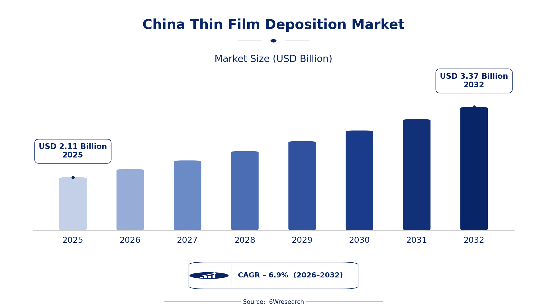
According to 6Wresearch internal database and industry insights, the China Thin Film Deposition Market was valued at USD 2.11 billion in 2025 and is projected to reach USD 3.37 billion by 2032, growing at a CAGR of approximately 6.9% during 2026–2032.
China Thin Film Deposition Market Highlights
| Report Metric | Details |
| Report Name | China Thin Film Deposition Market |
| Market Size 2025 | USD 2.11 billion |
| Market Size 2032 | USD 3.37 billion |
| Absolute Growth 2025–2032 | USD 1.26 billion |
| CAGR 2026–2032 | 6.9% |
| Peak Annual Growth | 9.4% in 2026 |
| Forecast Period | 2026–2032 |
| Historical Data | 2022–2025 |
| Base Year | 2025 |
| Leading Deposition Type, 2025 | Chemical Vapor Deposition (CVD) (37% share) |
| Leading Material Type, 2025 | Metals (42% share) |
| Leading Technology Used, 2025 | Sputtering (41% share) |
| Leading End User, 2025 | Semiconductor Foundries (48% share) |
| Fastest-Growing Deposition Type | Atomic Layer Deposition (ALD) (8.1% CAGR) |
| Fastest-Growing Material Type | Nanolayers (8.3% CAGR) |
| Fastest-Growing Technology Used | Plasma-Enhanced (9.1% CAGR) |
| Fastest-Growing End User | Solar Cell Firms (9.2% CAGR) |
| Growing Sector | Semiconductor Manufacturing |
| Key End Users | Semiconductor Foundries, Solar Cell Firms, Display Panel Producers |
China Thin Film Deposition Market Year-wise Growth Rate and Key Drivers (2022–2032)
This graph illustrates the annual growth rates of the market from 2022 to 2032, highlighting a steady upward trajectory and projected market expansion over the forecast period.
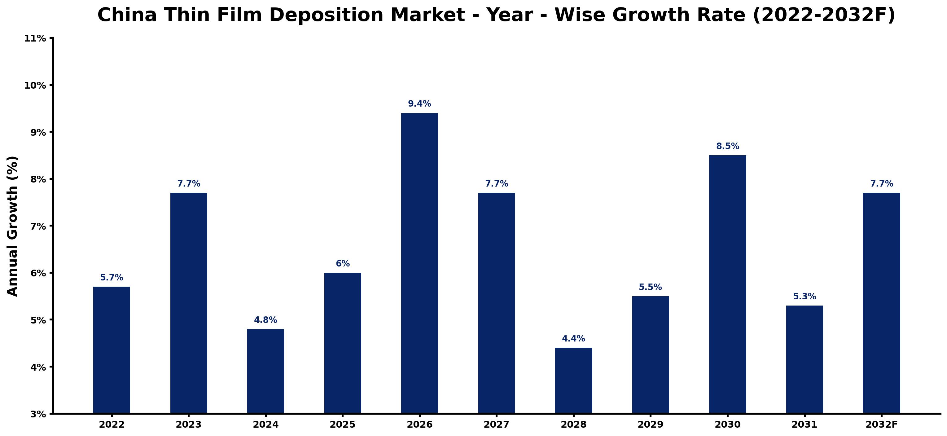
The table below sets out the estimated growth rate for each year and the main factor behind it.
| Year | Estimated Annual Growth (%) | Market Rationale |
| 2022 | 5.7 | The market experienced steady growth due to ongoing semiconductor production. |
| 2023 | 7.7 | Demand surged as the semiconductor industry expanded in key regions like Beijing and Shanghai. |
| 2024 | 4.8 | Growth slowed as market adjustments took place following rapid increases in previous years. |
| 2025 | 6.0 | A resurgence in investment in semiconductor technologies led to faster growth. |
| 2026 | 9.4 | The market peaked with significant advancements in thin film deposition technologies. |
| 2027 | 7.7 | Demand growth slowed as the market began to stabilise after the peak. |
| 2028 | 4.4 | Continued demand from semiconductor foundries contributed to slower growth rates. |
| 2029 | 5.5 | Growth picked up again as new applications in solar cells emerged. |
| 2030 | 8.5 | Investment in advanced deposition technologies drove further growth in the market. |
| 2031 | 5.3 | A slowdown occurred as the market adjusted to previous high growth rates. |
| 2032 | 7.7 | The market rebounded with renewed interest in semiconductor manufacturing. |
Note: Market size estimations and growth projections presented in this report are based on 6Wresearch's proprietary forecasting methodology, utilizing the latest available industry data, government publications, and primary research inputs.
China Thin Film Deposition Market Synopsis
Thin Film Deposition in China involves applying thin layers of material onto substrates, which is crucial for semiconductor manufacturing, display technology, and solar cells. The market is growing, propelled by substantial investments in the semiconductor sector, especially in regions like Beijing and Shanghai. With the semiconductor industry valued at around $200 billion, the demand for thin film deposition technologies is set to increase. Government initiatives, including the Integrated Circuit Industry Development Action Plan, further boost local production capabilities, ensuring ongoing growth in this market.
Market Dynamics Impact Analysis (2026–2032)
| Factor | Type | Impact | Primary Segment Affected |
| Increasing investments in semiconductor manufacturing capabilities | Driver | High | Chemical Vapor Deposition (CVD) |
| Rising demand for advanced materials in electronics | Driver | High | Nanolayers |
| Growing need for high-quality coatings in solar cell production | Opportunity | High | Solar Cell Firms |
| Expansion of semiconductor foundries in key regions | Opportunity | High | Semiconductor Foundries |
| Supply chain disruptions affecting material availability | Restraint | Medium | Physical Vapor Deposition (PVD) |
| High initial investment costs for advanced deposition technologies | Restraint | Medium | Atomic Layer Deposition (ALD) |
| Limited access to advanced technology for smaller firms | Challenge | High | Electrochemical Deposition |
| Competition from international manufacturers with advanced capabilities | Challenge | High | Sputtering |
Evaluation of Drivers in China Thin Film Deposition Market (2026–2032)
The main growth drivers and the segments they affect most are set out below.
| Drivers | Primary Segment Affected | Why It Matters (Evidence) |
| Rising semiconductor production | Physical Vapor Deposition (PVD) | The production of over 1.3 billion semiconductor chips in 2022 increases the demand for PVD technologies, essential for creating thin films in semiconductor manufacturing. |
| Growing solar cell production | Chemical Vapor Deposition (CVD) | With solar cell production reaching 150 GW in 2022, CVD technology is increasingly required for high-quality photovoltaic cell manufacturing. |
| Investment in advanced technologies | Atomic Layer Deposition (ALD) | The shift towards advanced semiconductor applications drives investment in ALD, which is crucial for precise layer control in next-generation devices. |
| Government funding initiatives | Sputtering | The National Semiconductor Industry Investment Fund, with a budget of $29 billion, supports the development of sputtering technologies, enhancing local manufacturing capabilities. |
| Increased R&D activities | Nanolayers | Research institutions published over 1,000 papers on thin film deposition in 2022, fostering innovation in nanolayer applications for advanced electronics. |
Expansion of the Thin Film Deposition market in China is backed by rising production of semiconductor chips and growing applications in solar energy. In 2022, China produced over 1.3 billion semiconductor chips, which drives the need for advanced technologies. The solar cell sector is also thriving, with production reaching 150 GW, leading to increased demand for thin film deposition. Investment in advanced deposition technologies is essential for meeting the requirements of semiconductor applications.
Evaluation of Restraints in China Thin Film Deposition Market
The table below lists the restraints and the evidence behind each.
| Market Restraint | Primary Segment Affected | Why It Matters (Evidence) |
| Supply chain disruptions affecting material availability | Physical Vapor Deposition (PVD) | Disruptions have led to shortages of essential materials, impacting production timelines and costs. |
| High initial investment costs for advanced deposition technologies | Atomic Layer Deposition (ALD) | The capital required for advanced equipment limits accessibility for smaller firms. |
| Limited access to advanced technology for smaller firms | Electrochemical Deposition | Many smaller manufacturers struggle to invest in the latest technologies, hindering their competitiveness. |
| Competition from international manufacturers with advanced capabilities | Sputtering | Local manufacturers face challenges from international firms that offer superior technologies and efficiencies. |
| Regulatory hurdles in the semiconductor sector | Chemical Vapor Deposition (CVD) | Strict regulations can delay project approvals, impacting timely market entry. |
China Thin Film Deposition Market Challenges
The China Thin Film Deposition Market encounters several practical issues, starting with a skills shortage that hampers production efficiency for semiconductor manufacturers. This challenge stems from a lack of specialised training programmes, resulting in project delays that can extend timelines by up to 20%. Rising raw material costs further complicate matters, increasing production expenses by 15%, which directly affects profit margins for producers. Outdated technology also presents challenges, as many facilities still depend on legacy systems, leading to a 20% decrease in output quality. Buyers face difficulties managing inventory due to fluctuating semiconductor production levels, complicating operations and raising costs.
Trends in the China Thin Film Deposition Market
Four trends stand out in the China Thin Film Deposition Market.
- Shift towards Advanced Materials in Semiconductor Manufacturing: China is increasingly prioritising advanced materials for semiconductor manufacturing, particularly in regions like Beijing. The demand for high-quality coatings is expected to rise, with the semiconductor industry valued at around $200 billion.
- Transition from Traditional to Modern Deposition Techniques: The market is shifting towards modern deposition techniques, such as Atomic Layer Deposition, which offers precise control. This transition is driven by the need for advanced semiconductor applications, with a projected CAGR of 8.1%.
- Emergence of Solar Cell Firms as Key End Users: Solar Cell Firms are becoming key consumers of thin film deposition technologies in China. With solar cell production reaching 150 GW in 2022, this trend is likely to persist as demand for renewable energy increases.
- Increase in Research and Development Activities: Research institutions in China published over 1,000 papers on thin film deposition in 2022. This surge in R&D activities reflects a growing interest in advancing deposition technologies within the semiconductor sector.
Investment Opportunities in the China Thin Film Deposition Market
Several openings in the China Thin Film Deposition Market merit attention from investors.
- Investment in Advanced Deposition Technologies: The demand for advanced deposition technologies is increasing, with China aiming for 70% self-sufficiency in semiconductor manufacturing by 2025. Investing in technologies like CVD can meet the needs of semiconductor foundries.
- Supply of High-Quality Coatings for Solar Cells: With solar cell production reaching 150 GW, there is a substantial opportunity to supply high-quality coatings. Solar Cell Firms are looking for reliable suppliers to fulfil their production requirements.
- Collaboration with Semiconductor Foundries: Engaging with Semiconductor Foundries in regions like Beijing and Shanghai presents a promising opportunity. Establishing partnerships can enhance market presence and provide access to advanced technologies.
- Development of Niche Applications in Electronics: The rise of niche applications in electronics, particularly in nanolayers, presents an opportunity. Focusing on these specialised markets can yield high returns for suppliers.
Government Initiatives in the China Thin Film Deposition Market
The Integrated Circuit Industry Development Action Plan, launched in 2021 by the Ministry of Industry and Information Technology, aims to improve domestic semiconductor production capabilities. This initiative focuses on increasing local manufacturing and reducing reliance on imports. The plan sets ambitious targets for self-sufficiency in semiconductor technologies, aiming for 70% self-sufficiency by 2025. Additionally, the '14th Five-Year Plan' emphasises advancements in semiconductor technology and materials, further supporting the growth of the thin film deposition market.
The National Development and Reform Commission oversees the Semiconductor Industry Investment Fund, approved in 2020 to support local manufacturers. This fund provides financial assistance for projects aimed at enhancing semiconductor production capabilities. Furthermore, the Ministry of Science and Technology introduced the National Key R&D Program in 2022, focusing on advanced semiconductor materials and technologies. These initiatives are crucial for driving innovation and development within the thin film deposition sector.
Future Insight of the China Thin Film Deposition Market
The China Thin Film Deposition Market will undergo substantial changes by 2032, supported by government initiatives and technological advancements. The Integrated Circuit Industry Development Action Plan aims to boost local production capabilities, contributing to a target of 70% self-sufficiency in semiconductor manufacturing by 2025. The National Semiconductor Industry Investment Fund, with a budget of $29 billion, will facilitate investments in modern facilities, strengthening supply chain resilience. Research institutions are expected to maintain their contributions, with over 1,000 papers on thin film deposition published in 2022, driving innovation for buyers and suppliers.
Market Segmentation Analysis
Each segment group is reviewed below, with the leader by share and the fastest grower by CAGR.
By Deposition Type – Chemical Vapor Deposition (CVD) Dominated, Atomic Layer Deposition (ALD) Expected to Grow Fastest
According to Vasudha, AM at 6Wresearch, the largest deposition type category in 2025 was Chemical Vapor Deposition (CVD), with a 37% share of total revenue. Chemical Vapor Deposition (CVD) holds the largest market share in China, largely due to its critical function in producing high-quality semiconductor materials and coatings. With the production of over 1.3 billion semiconductor chips in 2022, CVD is indispensable for meeting the industry's demands. The quickest growth will come from Atomic Layer Deposition (ALD), forecast to expand at a CAGR of 8.1% between 2026 and 2032. Atomic Layer Deposition (ALD) is experiencing rapid growth, driven by its importance in achieving precise layer control for advanced semiconductor applications. The increasing complexity of semiconductor designs is pushing manufacturers to adopt ALD technology, thereby accelerating its demand. Suppliers should focus on enhancing their CVD and ALD technologies to capture the expanding market share in China's semiconductor sector.
By Material Type – Metals Dominated, Nanolayers Expected to Grow Fastest
In 2025, Metals led the material type split with a 42% share. Metals dominate the market share as they are extensively used for conductive layers in electronics, which are vital for applications like semiconductors. This widespread use in the semiconductor industry solidifies their leading position in the market. Over 2026–2032, Nanolayers are expected to post the fastest growth, at a CAGR of 8.3%. Nanolayers are the fastest-growing segment, propelled by their critical role in advanced electronics and coatings that are increasingly required in high-tech applications. The ongoing trend towards miniaturisation in electronics is significantly driving this demand. Buyers should consider investing in nanolayer technologies to maintain competitiveness in the evolving electronics landscape.
By Technology Used – Sputtering Dominated, Plasma-Enhanced Expected to Grow Fastest
With a 41% revenue share in 2025, Sputtering was the largest technology used category. Sputtering technology commands the largest market share as it is a fundamental method for depositing thin films across various industries, particularly in semiconductor manufacturing. Its reliability and versatility make it a preferred choice among manufacturers. Plasma-Enhanced is projected to grow fastest, at a CAGR of 9.1% during 2026–2032. Plasma-Enhanced technology is witnessing rapid growth due to its capability to deliver superior film quality in semiconductor applications, which are becoming increasingly demanding. The rising need for enhanced film characteristics is fuelling this segment's expansion. Suppliers must focus on innovation in sputtering and plasma-enhanced technologies to remain competitive in the thin film deposition market.
By End User – Semiconductor Foundries Dominated, Solar Cell Firms Expected to Grow Fastest
Semiconductor Foundries accounted for a 48% market share by end user in 2025. Semiconductor Foundries represent the largest market share as they are the primary consumers of thin film deposition technologies essential for chip production. The robust semiconductor industry in China reinforces their dominant position in this market. Solar Cell Firms are set to record the highest CAGR in this split, 9.2% over 2026–2032. Solar Cell Firms are the fastest-growing end user segment, driven by the rising global demand for photovoltaic cells. China's leadership in solar cell production is significantly contributing to this growth trajectory. Suppliers should target solar cell firms to capitalise on the expanding market share driven by renewable energy initiatives.
Key Attractiveness of the Report
- 10 Years of Market Numbers
- Historical Data Starting from 2022 to 2025
- Base Year 2025
- Forecast Data until 2032
- Key Performance Indicators Impacting the Market
- Major Upcoming Developments and Projects
Key Highlights of the Report:
- China Thin Film Deposition Market Outlook
- Market Size of China Thin Film Deposition Market, 2025
- Forecast of China Thin Film Deposition Market, 2032
- Historical Data and Forecast of China Thin Film Deposition Revenues & Volume for the Period 2022 - 2032F
- China Thin Film Deposition Market Trend Evolution
- China Thin Film Deposition Market Drivers and Challenges
- China Thin Film Deposition Price Trends
- China Thin Film Deposition Porter's Five Forces
- China Thin Film Deposition Industry Life Cycle
- Historical Data and Forecast of China Thin Film Deposition Market Revenues & Volume By Deposition Type for the Period 2022 - 2032F
- Historical Data and Forecast of China Thin Film Deposition Market Revenues & Volume By Physical Vapor Deposition (PVD) for the Period 2022 - 2032F
- Historical Data and Forecast of China Thin Film Deposition Market Revenues & Volume By Chemical Vapor Deposition (CVD) for the Period 2022 - 2032F
- Historical Data and Forecast of China Thin Film Deposition Market Revenues & Volume By Atomic Layer Deposition (ALD) for the Period 2022 - 2032F
- Historical Data and Forecast of China Thin Film Deposition Market Revenues & Volume By Electrochemical Deposition for the Period 2022 - 2032F
- Historical Data and Forecast of China Thin Film Deposition Market Revenues & Volume By Material Type for the Period 2022 - 2032F
- Historical Data and Forecast of China Thin Film Deposition Market Revenues & Volume By Metals for the Period 2022 - 2032F
- Historical Data and Forecast of China Thin Film Deposition Market Revenues & Volume By Ceramics for the Period 2022 - 2032F
- Historical Data and Forecast of China Thin Film Deposition Market Revenues & Volume By Nanolayers for the Period 2022 - 2032F
- Historical Data and Forecast of China Thin Film Deposition Market Revenues & Volume By Conductive Inks for the Period 2022 - 2032F
- Historical Data and Forecast of China Thin Film Deposition Market Revenues & Volume By Technology Used for the Period 2022 - 2032F
- Historical Data and Forecast of China Thin Film Deposition Market Revenues & Volume By Sputtering for the Period 2022 - 2032F
- Historical Data and Forecast of China Thin Film Deposition Market Revenues & Volume By Plasma-Enhanced for the Period 2022 - 2032F
- Historical Data and Forecast of China Thin Film Deposition Market Revenues & Volume By Atomic Precision for the Period 2022 - 2032F
- Historical Data and Forecast of China Thin Film Deposition Market Revenues & Volume By Electrodeposition for the Period 2022 - 2032F
- Historical Data and Forecast of China Thin Film Deposition Market Revenues & Volume By End User for the Period 2022 - 2032F
- Historical Data and Forecast of China Thin Film Deposition Market Revenues & Volume By Semiconductor Foundries for the Period 2022 - 2032F
- Historical Data and Forecast of China Thin Film Deposition Market Revenues & Volume By Display Panel Producers for the Period 2022 - 2032F
- Historical Data and Forecast of China Thin Film Deposition Market Revenues & Volume By Solar Cell Firms for the Period 2022 - 2032F
- Historical Data and Forecast of China Thin Film Deposition Market Revenues & Volume By R&D Labs for the Period 2022 - 2032F
- China Thin Film Deposition Import Export Trade Statistics
- Market Opportunity Assessment By Deposition Type
- Market Opportunity Assessment By Material Type
- Market Opportunity Assessment By Technology Used
- Market Opportunity Assessment By End User
- China Thin Film Deposition Top Companies Market Share
- China Thin Film Deposition Competitive Benchmarking By Technical and Operational Parameters
- China Thin Film Deposition Company Profiles
- China Thin Film Deposition Key Strategic Recommendations
Market Covered
Segments analysed in this report are listed below.
By Deposition Type
- Physical Vapor Deposition (PVD)
- Chemical Vapor Deposition (CVD)
- Atomic Layer Deposition (ALD)
- Electrochemical Deposition
By Material Type
- Metals
- Ceramics
- Nanolayers
- Conductive Inks
By Technology Used
- Sputtering
- Plasma-Enhanced
- Atomic Precision
- Electrodeposition
By End User
- Semiconductor Foundries
- Display Panel Producers
- Solar Cell Firms
- R&D Labs